
Page 50 - Rashid, Power Electronics Handbook
P. 50
3 Thyristors 35
completing its turn-off cycle. Also, during turn-off, the power
dissipation can become excessive if the current and voltage are
simultaneously too large. Both of these turn-off problems can
damage the device as well as other portions of the circuit.
Another switching problem that occurs is associated
primarily with thyristors, although other power electronic
devices suffer some degradation of performance from the
same problem. This problem occurs because thyristors can
self-trigger into a forward-conduction mode from a forward-
blocking mode if the rate of rise of forward anode-cathode
voltage is too large. This triggering method is due to displace-
ment current through the associated junction capacitances
(capacitance at J dominates because it is reverse-biased under
2
forward applied voltage). The displacement current contri-
butes to the leakage current I , shown in Eq. (1). Therefore
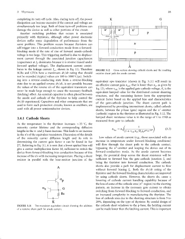
co FIGURE 3.12 Cross section showing cathode shorts and the resulting
SCRs and GTOs have a maximum dn=dt rating that should resistive shunt path for anode current.
not be exceeded (typical values are 100 to 1000 V=ms). Switch-
ing into a reverse-conducting state from a reverse-blocking
equivalent npn transistor (shown in Fig. 3.11) will result in
state due to an applied reverse dn=dt, is not possible because an effective current gain a that is lower than a , as given by
neff
n
the values of the reverse a's of the equivalent transistors can Eq. (2), where n is the applied gate-cathode voltage, R is the
never be made large enough to cause the necessary feedback GK s
equivalent lumped value for the distributed current shunting
(latching) effect. An external capacitor is often placed between
structure, and the remaining factors form the appropriate
the anode and cathode of the thyristor to help control the
current factor based on the applied bias and characteristics
dn=dt experienced. Capacitors and other components that are
of the gate-cathode junction. The shunt current path is
used to form such protection circuits, known as snubbers, are
implemented by providing intermittent shorts, called cathode
used with all power semiconductor devices. þ
shorts, between the p-base (gate) region and the n -emitter
(cathode) region in the thyristor as illustrated in Fig. 3.12. The
3.4.1 Cathode Shorts lumped shunt resistance value is in the range of 1 to 15 O as
measured from gate to cathode.
As the temperature in the thyristor increases >25 C, the
minority carrier lifetime and the corresponding diffusion a ¼ a 1 ð3:2Þ
lengths in the n- and p-bases increase. This leads to an increase n eff n 1 þ n GK n S 0 qn GK =kT
a =R i e
in the a's of the equivalent transistors. Discussion of the details
of the minority carrier diffusion length and its role in Low values of anode current (e.g., those associated with an
determining the current gain factor a can be found in Sze increase in temperature under forward-blocking conditions)
[7]. Referring to Eq. (1), it is seen that a lower applied bias will will ¯ow through the shunt path to the cathode contact,
þ
give a carrier multiplication factor M, suf®cient to switch the bypassing the n -emitter and keeping the device out of its
device from forward-blocking into conduction because of this forward-conduction mode. As the anode current becomes
increase of the a's with increasing temperature. Placing a shunt large, the potential drop across the shunt resistance will be
resistor in parallel with the base-emitter junction of the suf®cient to forward bias the gate-cathode junction J and
3
bring the thyristor into forward conduction. The cathode
shorts also provide a path for displacement current to ¯ow
without forward biasing J . Both the dn=dt rating of the
3
thyristor and the forward blocking characteristics are improved
by using cathode shorts. However, the shorts do, cause a
lowering of cathode current handling capability because of
þ
the loss of some of the cathode area (n -region) to the shorting
pattern, an increase in the necessary gate current to obtain
switching from forward-blocking to forward-conduction, and
an increased complexity in manufacturing the thyristor. The
loss of cathode area due to the shorting-structure is from 5 to
20%, depending on the type of thyristor. By careful design of
FIGURE 3.11 Two-transistor equivalent circuit showing the addition the cathode short windows to the p-base, the holding current
of a resistive shunt path for anode current. can be made lower than the latching current. This is important