
Page 45 - Rashid, Power Electronics Handbook
P. 45
J. Hudgins et al.
3030 J. Hudgins et al.
result in signi®cant carrier multiplication, denoted as a multi- thus interrupting base current to the pnp transistor and
plying factor M on the current components I and i . causing thyristor turn-off. This is similar in principle to
G
co
using negative base current to quickly turn off a traditional
MI þ Ma i transistor.
co
n G
i ¼ ð3:1Þ
A
1 ÿ Mða þ a Þ
p
n
3.3 Static Characteristics
In the forward-blocking state, the leakage current I co is
small, both a's are small, and their sum is < unity. Gate 3.3.1 Current-Voltage Curves for Thyristors
current increases the current in both transistors, increasing
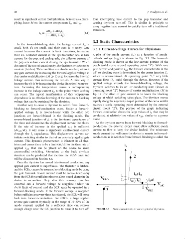
their a's. Collector current in the npn transistor acts as base A plot of the anode current (i ) as a function of anode-
A
current for the pnp, and analogously, the collector current of cathode voltage (n AK ) is shown in Fig. 3.3. The forward-
the pnp acts as base current driving the npn transistor. When blocking mode is shown as the low-current portion of the
the sum of the two a's equals unity, the thyristor switches to its graph (solid curve around operating point ‘‘1''). With zero
on-state (latches). This condition can also be reached, without gate current and positive n AK the forward characteristic in the
any gate current, by increasing the forward applied voltage so off- or blocking-state is determined by the center junction J ,
2
that carrier multiplication (M 1) at J increases the internal which is reverse-biased. At operating point ‘‘1,'' very little
2
leakage current, thus increasing the two a's. A third way to current ¯ows (I co only) through the device. However, if the
increase the a's is by increasing the device (junction) tempera- applied voltage exceeds the forward-blocking voltage, the
ture. Increasing the temperature causes a corresponding thyristor switches to its on- or conducting-state (shown as
increase in the leakage current I to the point where latching operating point ‘‘2") because of carrier multiplication (M in
co
can occur. The typical manifestation of this temperature Eq. 1). The effect of gate current is to lower the blocking
dependence is an effective lowering of the maximum blocking voltage at which switching takes place. The thyristor moves
voltage that can be sustained by the thyristor. rapidly along the negatively sloped portion of the curve until it
Another way to cause a thyristor to switch from forward- reaches a stable operating point determined by the external
blocking to forward-conduction exists. Under a forward- circuit (point ‘‘2"). The portion of the graph indicating
applied voltage, J 2 is reverse-biased while the other two forward conduction shows the large values of i that may be
A
junctions are forward-biased in the blocking mode. The conducted at relatively low values of n AK , similar to a power
reverse-biased junction of J is the dominant capacitance of diode.
2
the three and determines the displacement current that ¯ows. As the thyristor moves from forward-blocking to forward-
If the rate of increase in the applied n AK is suf®cient conduction, the external circuit must allow suf®cient anode
(dn AK =dt), it will cause a signi®cant displacement current current to ¯ow to keep the device latched. The minimum
through the J capacitance. This displacement current can anode current that will cause the device to remain in forward-
2
initiate switching similar to that of an externally applied gate conduction as it switches from forward-blocking is called the
current. This dynamic phenomenon is inherent in all thyr-
istors and causes there to be a limit (dn=dt) to the time rate of i A
applied n that can be placed on the device to avoid
AK
uncontrolled switching. Alterations to the basic thyristor
structure can be produced that increase the dn=dt limit and 2
will be discussed in Section 3.4.
Once the thyristor has moved into forward conduction, any
applied gate current is super¯uous. The thyristor is latched,
and for SCRs, cannot be returned to a blocking mode by using
the gate terminal. Anode current must be commutated away I I >I G1
G2
from the SCR for a suf®cient time to allow stored charge in the V L
device to recombine. Only after this recovery time has RBD I H I G2 I G1 I =0
G
occurred can a forward voltage be reapplied (below the V AK
dn=dt limit of course) and the SCR again be operated in a 3 1 V
forward-blocking mode. If the forward voltage is reapplied FBD
before suf®cient recovery time has elapsed, the SCR will move
back into forward-conduction. For GTOs, a large applied
reverse gate current (typically in the range of 10–50% of the
anode current) applied for a suf®cient time can remove
enough charge near the GK junction to cause it to turn off, FIGURE 3.3 Static characteristic i-n curve typical of thyristors.