
Page 47 - Rashid, Power Electronics Handbook
P. 47
et
Hudgins
J.
3232 J. Hudgins et al.
al.
n + ii) good thermal performance;
p iii) good electrical performance;
iv) long life=high reliability; and
n - v) low cost.
Electrical isolation of the baseplate from the semiconductor is
necessary in order to contain both halves of a phase leg in one
package as well as for convenience (modules switching to
p different phases can be mounted on one heat sink) and safety
(heat sinks can be held at ground potential).
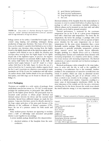
FIGURE 3.6 Cross section of a thyristor showing the negative bevel Thermal performance is measured by the maximum
þ
ÿ
ÿ
(upper pn - and pn -junctions) and positive bevel (lower pn -junction)
temperature rise in the Si die at a given power dissipation
used for edge termination of large-area devices.
level with a ®xed heat sink temperature. The lower the die
temperature, the better the package. A package with a low
leakage current at the surface. Controlled bevel angles can be thermal resistance from junction-to-sink can operate at higher
created using lapping and polishing techniques during power densities for the same temperature rise or lower
production of large-area thyristors. Two types of bevel junc- temperatures for the same power dissipation than a more
tions can be created: i) a positive bevel de®ned as one in which thermally resistive package. While maintaining low device
the junction area decreases when moving from the highly temperature is generally preferable, temperature variation
doped to the lightly doped side of the depletion region; and ii) affects majority carrier and bipolar devices differently.
a negative bevel de®ned as one in which the junction area Roughly speaking, in a bipolar device such as a thyristor,
increases when moving from the highly doped to the lightly switching losses increase and conduction losses decrease with
doped side of the depletion region. In practice, the negative increasing temperature. In a majority carrier device, conduc-
bevel must be lapped at an extremely shallow angle to reduce tion losses increase with increasing temperature. The thermal
the surface ®eld below the ®eld intensity in the bulk. All conductivity of typical materials used in thyristor packages is
positive bevel angles between 0 and 90 result in a lower shown in Table 3.1.
surface ®eld than in the bulk. Figure 3.6 shows the use of a Electrical performance refers primarily to the stray induc-
positive bevel for the J junction and a shallow negative bevel tance in series with the die, as well as the capability of
1
for the J and J junctions on a thyristor cross section to make mounting a low-inductance bus to the terminals. Another
2
3
maximum use of the Si area for conduction and still reduce problem is the minimization of capacitive crosstalk from one
the surface electric ®eld. Further details of the use of beveling, switch to another, which can cause an abnormal on-state
®eld plates, and ®eld rings can be found in Ghandi [2] and condition by charging the gate of an off-state switch, or
Baliga [3]. from a switch to any circuitry in the package Ð as would be
found in a hybrid power module. Capacitive coupling is a
major cause of electromagnetic interference (EMI). As the
3.3.3 Packaging
stray inductance of the module and the bus sets a minimum
Thyristors are available in a wide variety of packages, from switching loss for the device because the switch must absorb
small plastic ones for low-power (i.e., TO-247), to stud-mount the stored inductive energy, it is very important to minimize
packages for medium-power, to press-pack (also called ¯at-
pack) for the highest power devices. The press-packs must be
mounted under pressure to obtain proper electrical and
thermal contact between the device and the external metal TABLE 3.1 Thermal conductivity of thyristor package materials
electrodes. Special force-calibrated clamps are made for this
Thermal Conductivity
purpose. Large-area thyristors cannot be directly attached to Material ðW=m KÞ at 300 K
the large copper pole-piece of the press-pack because of the
Silicon 150
difference in the coef®cient of thermal expansion (CTE),
Copper (baseplate and pole pieces) 390–400
hence the use of a pressure contact for both anode and AlN substrate 170
cathode. Al 2 O 3 (Alumina) 28
Many medium-power thyristors are appearing in modules Aluminum (Al) 220
Tungsten (W) 167
where a half- or full-bridge (and associated anti-parallel
Molybdenum (Mo) 138
diodes) is put together in one package.
Metal matrix composites (MMC) 170
A power module package should have ®ve characteristics: Thermal grease (heatsink compound) 0.75
60=40 Solder (Pb=Sn eutectic) 50
i) electrical isolation of the baseplate from the semi-
95=5 Solder (Pb=Sn high temperature) 35
conductor;