
Page 49 - Rashid, Power Electronics Handbook
P. 49
Hudgins
J.
et
3434 J. Hudgins et al.
al.
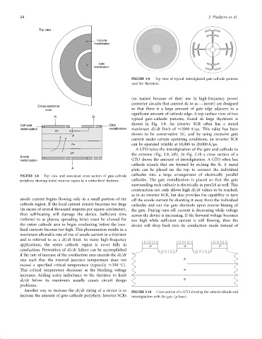
Top view
Cathode
metallization
Gate
metallization
FIGURE 3.9 Top view of typical interdigitated gate-cathode patterns
used for thyristors.
(so named because of their use in high-frequency power
converter circuits that convert dc to ac Ð invert) are designed
Cross-sectional
view so that there is a large amount of gate edge adjacent to a
signi®cant amount of cathode edge. A top surface view of two
K G
typical gate-cathode patterns, found in large thyristors is
Cathode Gate shown in Fig. 3.9. An inverter SCR often has a stated
metallization n+ metallization maximum di=dt limit of 2000 A=ms. This value has been
shown to be conservative [6], and by using excessive gate
p
current under certain operating conditions, an inverter SCR
n– can be operated reliably at 10,000 to 20,000 A=ms.
A GTO takes the interdigitation of the gate and cathode to
p+
Anode the extreme (Fig. 3.9, left). In Fig. 3.10 a cross section of a
metallization GTO shows the amount of interdigitation. A GTO often has
cathode islands that are formed by etching the Si. A metal
A
plate can be placed on the top to connect the individual
cathodes into a large arrangement of electrically parallel
FIGURE 3.8 Top view and associated cross section of gate-cathode
periphery showing initial turn-on region in a center-®red thyristor. cathodes. The gate metallization is placed so that the gate
surrounding each cathode is electrically in parallel as well. This
construction not only allows high di=dt values to be reached,
as in an inverter SCR, but also provides the capability to turn
anode current begins ¯owing only in a small portion of the off the anode current by shunting it away from the individual
cathode region. If the local current density becomes too large cathodes and out the gate electrode upon reverse-biasing of
(in excess of several thousand amperes per square centimeter), the gate. During turn-off, current is decreasing while voltage
then self-heating will damage the device. Suf®cient time across the device is increasing. If the forward voltage becomes
(referred to as plasma spreading time) must be allowed for too high while suf®cient current is still ¯owing, then the
the entire cathode area to begin conducting before the loca- device will drop back into its conduction mode instead of
lized currents become too high. This phenomenon results in a
maximum allowable rate of rise of anode current in a thyristor
and is referred to as a di=dt limit. In many high-frequency
applications, the entire cathode region is never fully in n + n + n +
conduction. Prevention of di=dt failure can be accomplished
if the rate of increase of the conduction area exceeds the di=dt p
rate such that the internal junction temperature does not
exceed a speci®ed critical temperature (typically 350 C).
This critical temperature decreases as the blocking voltage n -
increases. Adding series inductance to the thyristor to limit p
di=dt below its maximum usually causes circuit design
problems.
Another way to increase the di=dt rating of a device is to FIGURE 3.10 Cross section of a GTO showing the cathode islands and
increase the amount of gate-cathode periphery. Inverter SCRs interdigitation with the gate (p-base).