
Page 54 - Rashid, Power Electronics Handbook
P. 54
3 Thyristors 39
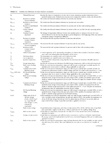
TABLE 3.5 Symbols and de®nitions of major thyristor parameters
R y Thermal Resistance Speci®es the degree of temperature rise per unit of power, measuring junction temperature from a
speci®ed external point. De®ned when junction power dissipation results in steady-state thermal ¯ow.
Junction-to-ambient The steady-state thermal resistance between the junction and ambient.
R yðJÿAÞ
thermal resistance
Junction-to-case thermal The steady-state thermal resistance between the junction and case surface.
R yðJÿCÞ
resistance
Junction-to-sink thermal The steady-state thermal resistance between the junction and the heat sink mounting surface.
R yðJÿSÞ
resistance
Contact thermal The steady-state thermal resistance between the surface of the case and the heat sink mounting surface.
R yðCÿSÞ
resistance
Transient thermal The change of temperature difference between two speci®ed points or regions at the end of a time
Z y
impedance interval divided by the step function change in power dissipation at the beginning of the same interval
causing the change of temperature difference.
Junction-to-ambient The transient thermal impedance between the junction and ambient.
Z yðJÿAÞ
transient thermal
impedance
Junction-to-case transient The transient thermal impedance between the junction and the case surface.
Z yðJÿCÞ
thermal impedance
Junction-to-sink The transient thermal impedance between the junction and the heat sink mounting surface.
Z yðJÿSÞ
transient thermal
impedance
Ambient temperature It is the temperature of the surrounding atmosphere of a device when natural or forced-air cooling is
T A
used, and is not in¯uenced by heat dissipation of the device.
Sink temperature The temperature at a speci®ed point on the device heat sink.
T S
Case temperature The temperature at a speci®ed point on the device case.
T C
Junction temperature The device junction temperature rating. Speci®es the maximum and minimum allowable operation
T J
temperatures.
Storage temperature Speci®es the maximum and minimum allowable storage temperatures (with no electrical connections).
T STG
Peak reverse blocking Within the rated junction temperature range, and with the gate terminal open-circuited, speci®es the
V RRM
voltage repetitive peak reverse anode to cathode voltage applicable on each cycle.
Transient peak reverse Within the rated junction temperature range, and with the gate terminal open-circuited, speci®es the
V RSM
blocking voltage nonrepetitive peak reverse anode to cathode voltage applicable for a time width equivalent to < 5 ms.
V RðDCÞ SCR Only DC Reverse blocking Within the rated junction temperature range, and with the gate terminal open-circuited, speci®es the
voltage maximum value for dc anode to cathode voltage applicable in the reverse direction.
V DRM Peak forward blocking Within the rated junction temperature range, and with the gate terminal open-circuited (SCR), or with a
voltage speci®ed reverse voltage between the gate and cathode (GTO), speci®es the repetitive peak off-state
anode to cathode voltage applicable on each cycle. This does not apply for transient off-state voltage
application.
Transient peak forward Within the rated junction temperature range, and with the gate terminal open-circuited (SCR), or with a
V DSM
blocking voltage speci®ed reverse voltage between the gate and cathode (GTO), speci®es the nonrepetitive off-state
anode to cathode voltage applicable for a time width equivalent to < 5 ms. This gives the maximum
instantaneous value for nonrepetitive transient off-state voltage.
DC Forward blocking Within the rated junction temperature range, and with the gate terminal open-circuited (SCR), or with a
V DðDCÞ
voltage speci®ed reverse voltage between the gate and cathode (GTO), speci®es the maximum value for dc
anode to cathode voltage applicable in the forward direction.
dn=dt Critical rate-of-rise of At the maximum rated junction temperature range, and with the gate terminal open-circuited (SCR), or
off-state voltage with a speci®ed reverse voltage between the gate and cathode (GTO), this speci®es the maximum rate-
dn=dt ¼ð0:632 V D Þ=t of-rise of off-state voltage that will not drive the device from an off-state to an on-state when an
V D is speci®ed off- exponential off-state voltage of speci®ed amplitude is applied to the device.
state voltage t is time
constant for
exponential
Peak on-state voltage At speci®ed junction temperature, and when on-state current (50 or 60 Hz, half sine wave of speci®ed
V TM
peak amplitude) is applied to the device, indicates peak-value for the resulting voltage drop.
RMS on-state current At speci®ed case temperature, indicates the rms value for on-state current that can be continuously
I TðRMSÞ
applied to the device.
Average on-state current At speci®ed case temperature, and with the device connected to a resistive or inductive load, indicates
I TðAVÞ
the average value for forward-current (sine half wave, commercial frequency) that can be continuously
applied to the device.
Peak on-state current Within the rated junction temperature range, indicates the peak-value for non-repetitive on-state current
I TSM
(sine half wave, 50 or 60 Hz). This value indicated for one cycle, or as a function of a number of
cycles.
(continued )