
Page 57 - Rashid, Power Electronics Handbook
P. 57
et
Hudgins
J.
al.
4242 J. Hudgins et al.
tion capability. Both turn-on, which is relatively simple, by
comparison, and conduction properties approach the one- p +
dimensional (1D) thyristor limit. p +
Early generations of MCTs had >50,000 cells connected in
parallel. Newer devices have >200,000 cells, with a total active
2
area of 0:38 cm . These devices are rated for 1000 V and a peak cathode
controllable current of 75 A. All of the cells contain an n- n + n + n +
p p p
channel FET structure to turn off, and 4% have the p-channel
FET structure to turn the device on. The latest version of the gate
‘‘standard'' MCT is a diffusion–doped (instead of the usual oxide
2
epitaxial growth) device with an active area of 1 cm . They are
rated for 3000-V forward blocking, have a forward drop of
2.5 V at 100 A, and are capable of interrupting around 300 A
with a recovery time of 5 ms. Three of these high-voltage
devices have been placed in a series array that operates at 5- n +
kV blocking and interrupts 150 A. Other MCTs have been p +
designed to withstand 2.5 kV with a turn-off capability of anode
several kiloamperes per square centimeter per unit cell. Turn-
off simulations have been performed for high-voltage MCTs anode
as well as discussion of lateral device designs. A thorough
analysis of the interaction of ®eld plates and guard rings
in punch-through and non-punch-through structures, for
achieving high-voltage planar junctions has also been gate
performed.
Trench- or buried-gate technology has contributed to the
reduction of the R on Area product in power MOSFETs by a
factor of three or more compared to surface gate devices. An
MCT that uses this technology, called a depletion-mode
thyristor (DMT), was designed. The cross section of the
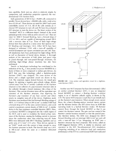
device and a simple equivalent circuit are shown in Fig. cathode
3.18. The depletion region formed between the trench-gate FIGURE 3.18 Cross section and equivalent circuit for a depletion-
®ngers, by applying a negative gate-cathode voltage, diverts mode thyristor (DMT).
þ
current away from the n -emitter (cathode) of the thyristor
structure to the collector of a pnp transistor structure (also at
the cathode) through a lateral resistance (the p-base of the Another new MCT structure has been demonstrated. Called
thyristor). This current diversion turns off the equivalent npn an emitter switched thyristor (EST), it uses an integrated
transistor of the thyristor structure, thus depriving the lateral MOSFET to connect a ¯oating thyristor n-emitter
þ
thyristor's pnp transistor of any base current and which region to an n -thyristor cathode region, as shown in Fig.
results in complete turn-off of the device. Depletion mode 3.19. The lateral MOS structure is such that it can initially turn
thyristors were produced that had forward-blocking ratings of on the thyristor's pnp transistor. When enough anode current
2
500 V, 1.1 V forward drop at 200 A=cm (a similar IGBT had ¯ows, the p-base-n-¯oating-emitter junction injects carriers
a forward drop of 2 V at the same current density), and could and the thyristor latches (the EST moves from an IGBT-like
2
control a maximum current density of 5000 A=cm . A similar operating mode to a latched thyristor mode). All thyristor
device is the base resistance controlled thyristor (BRT). Here, current ¯ows through the lateral MOSFET so that it can
a p-channel MOSFET is integrated into the n-drift region of control the thyristor current. The gate can lose control if the
the MCT, and is used to modulate the lateral p-base resis- thyristor current becomes excessive so that the parallel para-
tance of the thyristor, causing the holding current to increase sitic thyristor latches. The ESTs were designed for 600-V
2
above the conduction value, thus achieving turn-off. Some forward-blocking and can interrupt 1000 A=cm per unit cell
BRTs were fabricated with 600-V blocking capability and an with a turn-off time 7 ms. Integrating an IGBT into a
2
active area of 1:3mm (315 cells). These devices operate in thyristor structure has been proposed. This device, called an
an ‘‘IGBT'' mode until the current is large enough to cause IGBT-triggered thyristor (ITT), is similar in structure and
the thyristor structure to latch. The forward drop was 1.24 V operation to the EST. Two-dimensional (2D) simulations
2
at 300 A=cm , about the same as a similarly fabricated comparing switching of an inductive load and conduction
thyristor. performance of the ITT to a conventional IGBT have indicated