Page 60 - Rashid, Power Electronics Handbook
P. 60

3 Thyristors                                                                                         45

                                                    A


                                                                                         i
                                        n 3
                                 J 4                             p 1

                                                                    J 1
                                                                 n 1
                                                                     J 2                               v
                                                                 p 2
                                                                     J 3
                                                                 n 2


                                                    K
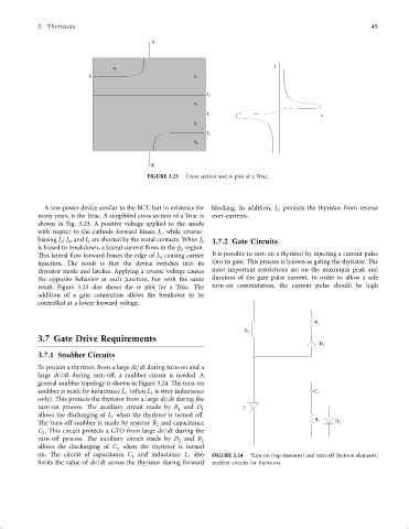
                                                  FIGURE 3.23  Cross section and iv plot of a Triac.


                   A low-power device similar to the BCT, but in existence for  blocking. In addition, L protects the thyristor from reverse
                                                                                          1
                 many years, is the Triac. A simpli®ed cross section of a Triac is  over-currents.
                 shown in Fig. 3.23. A positive voltage applied to the anode
                 with respect to the cathode forward-biases J , while reverse-
                                                      1
                 biasing J ; J , and J are shorted by the metal contacts. When J
                        2  4    3                                  2  3.7.2 Gate Circuits
                 is biased to breakdown, a lateral current ¯ows in the p -region.
                                                             2
                 This lateral ¯ow forward-biases the edge of J , causing carrier  It is possible to turn on a thyristor by injecting a current pulse
                                                      3
                 injection. The result is that the device switches into its  into its gate. This process is known as gating the thyristor. The
                 thyristor mode and latches. Applying a reverse voltage causes  most important restrictions are on the maximum peak and
                 the opposite behavior at each junction, but with the same  duration of the gate pulse current. In order to allow a safe
                 result. Figure 3.23 also shows the iv plot for a Triac. The  turn-on commutation, the current pulse should be high
                 addition of a gate connection allows the breakover to be
                 controlled at a lower forward voltage.


                                                                                                     R 1
                                                                                L 1
                 3.7 Gate Drive Requirements
                                                                                                      D 1
                 3.7.1 Snubber Circuits
                 To protect a thyristor, from a large di=dt during turn-on and a
                 large dv=dt during turn-off, a snubber circuit is needed. A
                 general snubber topology is shown in Figure 3.24. The turn-on
                 snubber is made by inductance L (often L is stray inductance                        C 2
                                            1
                                                    1
                 only). This protects the thyristor from a large di=dt during the
                 turn-on process. The auxiliary circuit made by R and D 1      T
                                                            1
                 allows the discharging of L when the thyristor is turned off.
                                        1
                                                                                                     R 2
                 The turn-off snubber is made by resistor R and capacitance                                D 2
                                                     2
                 C . This circuit protects a GTO from large dv=dt during the
                   2
                 turn-off process. The auxiliary circuit made by D and R 2
                                                            2
                 allows the discharging of C when the thyristor is turned
                                         2
                 on. The circuit of capacitance C and inductance L also  FIGURE 3.24  Turn-on (top elements) and turn-off (bottom elements)
                                              2
                                                               1
                 limits the value of dv=dt across the thyristor during forward  snubber circuits for thyristors.
   55   56   57   58   59   60   61   62   63   64   65