
Page 63 - Rashid, Power Electronics Handbook
P. 63
J. Hudgins et al.
4848 J. Hudgins et al.
i G
(a)
+
0 a p 2 p a p 2 p 3 w t
i G
(b )
a a
0 p 2 p + p 3 p w t
2
i G
(c)
a a w
0 p 2 p + p 3 p t
2
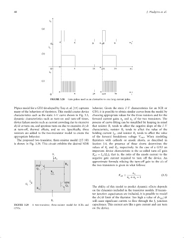
FIGURE 3.28 Gate pulses used as an alternative to one long current pulse.
PSpice model for a GTO developed by Tsay et. al. [13] captures behavior. Given the static I-V characteristics for an SCR or
many of the behaviors of thyristors. This model creates device GTO, it is possible to obtain similar curves from the model by
characteristics such as the static I-V curve shown in Fig. 3.3, choosing appropriate values for the three resistors and for the
dynamic characteristics such as turn-on and turn-off times, forward current gains a and a of the two transistors. The
n
p
device failure modes such as current crowding due to excessive process of curve-®tting can be simpli®ed by keeping in mind
di=dt at turn-on, and spurious turn-on due to excessive dn=dt that resistor R tends to affect the negative slope of the I-V
1
at turn-off, thermal effects, and so on. Speci®cally, three characteristic, resistor R tends to affect the value of the
2
resistors are added to the two-transistor model to create the holding current I , and resistor R tends to affect the value
H
3
appropriate behavior. of the forward breakdown voltage V FBD . When modeling
The proposed two-transistor, three-resistor model (2T-3R) thyristors with cathode or anode shorts, as described in
is shown in Fig. 3.29. This circuit exhibits the desired NDR Section 3.4, the presence of these shorts determines the
values of R and R , respectively. In the case of a GTO an
1
2
important device characteristic is the so-called turn-off gain
A i K off ¼ I =jI j, that is, the ratio of the anode current to the
G
A
I Ai negative gate current required to turn off the device. An
approximate formula relating the turn-off gain to the a's of
PNP R 2i the two transistors is given in what follows:
Q 1i
R 3i a
K off ¼ n ð3:3Þ
a þ a ÿ 1
p
n
I Gi NPN
G i
Q 2i
The ability of this model to predict dynamic effects depends
R 1i
on the dynamics included in the transistor models. If transis-
tor junction capacitances are included, it is possible to model
the dn=dt limit of the thyristor. Too high a value of dn AK =dt
K i will cause signi®cant current to ¯ow through the J junction
2
FIGURE 3.29 A two-transistor, three-resistor model for SCRs and capacitance. This current acts like a gate current and can turn
GTOs. on the device.