Page 64 - Rashid, Power Electronics Handbook
P. 64

3 Thyristors                                                                                         49


                                   GATE

                                  Islands
                                  (Cathode)

                                     Anode


                                     A1               A2            A3                                        A8
                                      Cell            Cell           Cell                                      Cell
                                     Model            Model         Model                                     Model
                                RGC1   1        RGC2   2       RGC3   3                                 RGC8    8
                                   G1   K1         G2   K2        G3  K3                                   G8   K8
                                   RKC1            RKC2           RKC3     ......................................  RKC8

                                                M 12          M 23

                                                 Delay
                                                                Delay
                                 Delay
                    Gate         Circuit         Circuit       Circuit

                                     Cathode
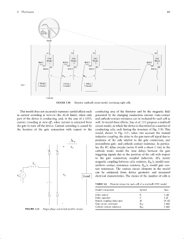
                                            FIGURE 3.30  Thyristor multicell circuit model containing eight cells.


                   This model does not accurately represent spatial effects such  conducting area of the thyristor and by the magnetic ®eld
                 as current crowding at turn-on (the di=dt limit), when only  generated by the changing conduction current. Gate-contact
                 part of the device is conducting, and, in the case of a GTO,  and cathode-contact resistance can be included for each cell as
                 current crowding at turn-off , when current is extracted from  well. To model these effects, Tsay et al. [13] propose a multicell
                 the gate to turn off the device. Current crowding is caused by  circuit model, in which the device is discretized in a number of
                 the location of the gate connection with respect to the  conducting cells, each having the structure of Fig. 3.30. This
                                                                      model, shown in Fig. 3.31, takes into account the mutual
                                                                      inductive coupling, the delay in the gate turn-off signal due to
                                                      i d             positions of the cells relative to the gate connection, and
                                                                      nonuniform gate- and cathode-contact resistance. In particu-
                                                +     L d             lar, the RC delay circuits (series R with a shunt C tied to the
                                                                      cathode node) model the time delays between the gate
                                                                      triggering signals due to the position of the cell with respect
                                                                      to the gate connection; coupled inductors, M's, model
                            L s                                       magnetic coupling between cells; resistors, R 's, model non-
                                                                                                          KC
                                                                      uniform contact resistance; resistors, R 's, model gate con-
                                                                                                      GC
                    +                                                 tact resistances. The various circuit elements in the model
                                                                      can be estimated from device geometry and measured
                  v s                           v d           Load    electrical characteristics. The choice of the number of cells is
                    -
                                                                      TABLE 3.6  Element values for each cell of a multicell GTO model
                                                                      Model Component               Symbol          Vaue
                                                                      Delay resistor                R               1 mO
                                                                      Delay capacitor               C               1 nF
                                                                      Mutual coupling inductance    M               10 nH
                                                -                     Gate contact resistance       R GC            1 mO
                                                                      Cathode contact resistance    R KC            1 mO
                       FIGURE 3.31  Single-phase controlled recti®er circuit.
   59   60   61   62   63   64   65   66   67   68   69