
Page 58 - Rashid, Power Electronics Handbook
P. 58
3 Thyristors 43
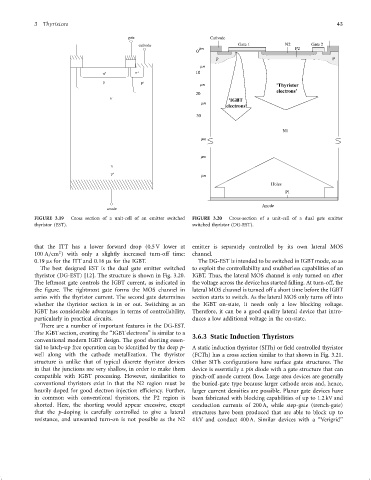
gate Cathode
cathode Gate 1 N2 Gate 2
0 m m P2
P P
m m
n + n + 10
p - p +
m m 'Thyristor
electrons'
20
n - 'IGBT
m m
electrons'
30
N1
m m
m m
n
p +
m m
Holes
P1
Anode
anode
FIGURE 3.19 Cross section of a unit-cell of an emitter switched FIGURE 3.20 Cross-section of a unit-cell of a dual gate emitter
thyristor (EST). switched thyristor (DG-EST).
that the ITT has a lower forward drop (0.5 V lower at emitter is separately controlled by its own lateral MOS
2
100 A=cm ) with only a slightly increased turn-off time: channel.
0:19 ms for the ITT and 0:16 ms for the IGBT. The DG-EST is intended to be switched in IGBTmode, so as
The best designed EST is the dual gate emitter switched to exploit the controllability and snubberless capabilities of an
thyristor (DG-EST) [12]. The structure is shown in Fig. 3.20. IGBT. Thus, the lateral MOS channel is only turned on after
The leftmost gate controls the IGBT current, as indicated in the voltage across the device has started falling. At turn-off, the
the ®gure. The rightmost gate forms the MOS channel in lateral MOS channel is turned off a short time before the IGBT
series with the thyristor current. The second gate determines section starts to switch. As the lateral MOS only turns off into
whether the thyristor section is in or out. Switching as an the IGBT on-state, it needs only a low blocking voltage.
IGBT has considerable advantages in terms of controllability, Therefore, it can be a good quality lateral device that intro-
particularly in practical circuits. duces a low additional voltage in the on-state.
There are a number of important features in the DG-EST.
The IGBT section, creating the ‘‘IGBT electrons'' is similar to a 3.6.3 Static Induction Thyristors
conventional modern IGBT design. The good shorting essen-
tial to latch-up free operation can be identi®ed by the deep p- A static induction thyristor (SITh) or ®eld controlled thyristor
well along with the cathode metallization. The thyristor (FCTh) has a cross section similar to that shown in Fig. 3.21.
structure is unlike that of typical discrete thyristor devices Other SITh con®gurations have surface gate structures. The
in that the junctions are very shallow, in order to make them device is essentially a pin diode with a gate structure that can
compatible with IGBT processing. However, similarities to pinch-off anode current ¯ow. Large area devices are generally
conventional thyristors exist in that the N2 region must be the buried-gate type because larger cathode areas and, hence,
heavily doped for good electron injection ef®ciency. Further, larger current densities are possible. Planar gate devices have
in common with conventional thyristors, the P2 region is been fabricated with blocking capabilities of up to 1.2 kV and
shorted. Here, the shorting would appear excessive, except conduction currents of 200 A, while step-gate (trench-gate)
that the p-doping is carefully controlled to give a lateral structures have been produced that are able to block up to
resistance, and unwanted turn-on is not possible as the N2 4 kV and conduct 400 A. Similar devices with a ‘‘Verigrid''