
Page 55 - Rashid, Power Electronics Handbook
P. 55
J. Hudgins et al.
4040 J. Hudgins et al.
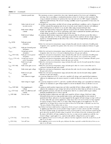
TABLE 3.5 (Continued)
2
I t Current-squared time The maximum, on-state, nonrepetitive short-time thermal capacity of the device and is helpful in
selecting a fuse or providing a coordinated protection scheme of the device in the equipment. This
rating is intended speci®cally for operation less than one half cycle of a 180 (degree) conduction
angle sinusoidal waveform. The off-state blocking capability cannot be guaranteed at values near the
2
maximum I t.
di=dt Critical rate-of-rise of At speci®ed case temperature, speci®ed off-state voltage, speci®ed gate conditions, and at a frequency of
on-state current <60 Hz, indicates the maximum rate-of-rise of on-state current which the thyristor will withstand
when switching from an off-state to an on-state, when using recommended gate drive.
I RRM Peak reverse leakage At maximum rated junction temperature, indicates the peak value for reverse-current ¯ow when a
current voltage (sine half wave, 50 or 60 Hz, and having a peak value as speci®ed for repetitive peak reverse-
voltage rating) is applied in a reverse direction to the device.
Peak forward leakage At maximum rated junction temperature, indicates the peak-value for off-state-current ¯ow when a
I DRM
current voltage (sine half wave, 50 or 60 Hz, and having a peak value for repetitive off-state voltage rating) is
applied in a forward direction to the device. For a GTO, a reverse voltage between the gate and
cathode is speci®ed.
P GM ðSCRÞ Peak gate power
dissipation Within the rated junction temperature range, indicates the peak value for maximum allowable power
dissipation over a speci®ed time period, when the device is in forward conduction between the gate
P GFM (GTO) Peak gate forward power and cathode.
dissipation
Average gate power Within the rated junction temperature range, indicates the average value for maximum allowable power
P GðAVÞ
dissipation dissipation when the device is forward-conducting between the gate and cathode.
P GRM GTO Only Peak gate reverse power Within the rated junction temperature range, indicates the peak value for maximum allowable power
dissipation dissipation in the reverse direction between the gate and cathode, over a speci®ed time period.
P GRðAVÞ GTO only Average gate reverse Within the rated junction temperature range, indicates the average value for maximum allowable power
power dissipation dissipation in the reverse direction between the gate and cathode.
Peak forward gate Within the rated junction temperature range, indicates the peak value for forward-current ¯ow between
I GFM
current the gate and cathode.
I GRM GTO Only Peak reverse gate current Within the rated junction temperature range, indicates peak value for reverse-current that can be
conducted between the gate and cathode.
Peak reverse gate voltage Within the rated junction temperature range, indicates the peak value for reverse-voltage applied between
V GRM
the gate and cathode.
Peak forward gate Within the rated junction temperature range, indicates the peak value for forward-voltage applied
V GFM
voltage between the gate and cathode.
I GT Gate current to trigger At a junction temperature of 25 C, and with a speci®ed off-voltage, and a speci®ed load resistance,
indicates the minimum gate dc current required to switch the thyristor from an off-state to an on-
state.
Gate voltage to trigger At a junction temperature of 25 C, and with a speci®ed off-state voltage, and a speci®ed load resistance,
V GT
indicates the minimum dc gate voltage required to switch the thyristor from an off-state to an on-
state.
V GDM SCR Only Nontriggering gate At maximum rated junction temperature, and with a speci®ed off-state voltage applied to the device,
voltage indicates the maximum dc gate voltage that will not switch the device from an off-state to an on-state.
I TGO GTO Only Gate controlled turn-off Under speci®ed conditions, indicates the instantaneous value for on-current usable in gate control,
current speci®ed immediately prior to device turn-off.
t on SCR Only Turn-on time At speci®ed junction temperature, and with a peak repetitive off-state voltage of half-rated value,
followed by device turn-on using speci®ed gate current, and when speci®ed on-state current of
speci®ed di=dt ¯ows, indicated as the time required for the applied off-state voltage to drop to 10% of
its initial value after gate current application. Delay time is the term used to de®ne the time required
for applied voltage to drop to 90% of its initial value following gate-current application. The time
required for the voltage level to drop from 90% to 10% of its initial value is referred to as rise time.
The sum of both of these de®nes turn-on time.
T q SCR Only Turn-off Time Speci®ed at maximum rated junction temperature. Device set up to conduct on-state current, followed
by applying speci®ed reverse anode-cathode voltage to quench on-state current, and then increasing
the anode-cathode voltage at a speci®ed rate-of-rise as determined by circuit conditions controlling the
point where the speci®ed off-state voltage is reached. Turn-off time de®nes the minimum time which
the device will hold its off-state, starting from the time on-state current reached zero until the time
forward voltage is again applied (i.e., applied anode-cathode voltage becomes positive again).
t gt GTO Only Turn-on time When applying forward-current to the gate, indicates the time required to switch the device from an off-
state to an on-state.
t qt GTO Only Turn-off time When applying reverse-current to the gate, indicates the time required to switch the device from an on-
state to an off-state.