
Page 56 - Rashid, Power Electronics Handbook
P. 56
3 Thyristors 41
during conduction, is removed. The associated displacement anode
current under application of forward voltage during the
thyristor blocking state sets a dn=dt limit. Some effort in oxide
improving the voltage hold-off capability and overvoltage gate
protection of conventional silicon-controlled recti®ers n + n +
(SCRs) is underway by incorporating a lateral high-resistivity p p
region to help dissipate the energy during break-over. Most p +
effort, though, is being directed toward further development
of high-performance gate turn-off (GTO) thyristors because of
their controllability and to a lesser extent in optically triggered n -
structures that feature gate circuit isolation.
High-voltage GTO thyristors with symmetric blocking
capability require thick n-base regions to support the high
þ
electric ®eld. The addition of an n -buffer layer next to the
þ
p -anode allows high voltage blocking and a low forward p -
voltage drop during conduction because of the thinner n-base
required. Cylindrical anode shorts have been incorporated to
facilitate excess carrier removal from the n-base during turn-
off and still retain high blocking capability. This device p
structure can control 200 A, operating at 900 Hz, with a 6- n +
kV hold-off. Some of the design trade-offs between the n-base
width and turn-off energy losses in these structures been
þ
determined. A similar GTO incorporating an n -buffer layer
and a pin structure has been fabricated that can control up to
1 kA (at a forward drop of 4 V) with a forward blocking
capability of 8 kV. A reverse-conducting GTO has been fabri- cathode
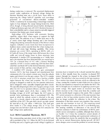
cated that can block 6 kV in the forward direction, interrupt a FIGURE 3.17 Cross section of unit-cell of a p-type MCT.
peak current of 3 kA, and has a turn-off gain of 5.
A modi®ed GTO structure, called a gate commutated
thyristor (GCT), has been designed and manufactured that inversion layer is formed in the n-doped material that allows
commutates all of the cathode current away from the cathode holes to ¯ow laterally from the p-emitter (p-channel FET
region and diverts it out the gate contact. The GCT is similar source) through the channel to the p-base (p-channel FET
to a GTO in structure except that it has a low-loss n-buffer drain). This hole ¯ow is the base current for the npn transistor.
region between the n-base and p-emitter. The GCT device The n-emitter then injects electrons, which are collected in the
package is designed to result in very low parasitic inductance n-base, causing the p-emitter to inject holes into the n-base so
and is integrated with a specially designed gate-drive circuit. that the pnp transistor is turned on and latches the MCT. The
The specially designed gate drive and ring-gate package circuit MCT is brought out of conduction by applying a positive gate-
allow the GCT to be operated without a snubber circuit and anode voltage. This signal creates an inversion layer that
switch with higher anode di=dt, than a similar GTO. At diverts electrons in the n-base away from the p-emitter and
blocking voltages of 4.5 kV and higher the GCT seems to into the heavily doped n-region at the anode. This n-channel
provide better performance than a conventional GTO. The FET current amounts to a diversion of the pnp transistor base
speed at which the cathode current is diverted to the gate current so that its base-emitter junction turns off. Holes are
(di GQ =dt) is directly related to the peak snubberless turn-off then no longer available for collection by the p-base. The
capability of the GCT. The gate drive circuit can sink current elimination of this hole current (npn transistor base current)
for turn-off at di GQ =dt values >7000 A=ms. This hard gate causes the npn transistor to turn off. The remaining stored
drive results in a low charge storage time of 1 ms. Low charge recombines and returns the MCT to its blocking state.
storage time and fail-short mode make the GCT attractive for The seeming variability in fabrication of the turn-off FET
high-voltage series applications. structure continues to limit the performance of MCTs, parti-
cularly current interruption capability, although these devices
can handle 2 to 5 times the conduction current density of
3.6.2 MOS-Controlled Thyristors, MCT
IGBTs. Numerical modeling and experimental veri®cation of
The corresponding equivalent circuit of the p-type MCT unit the modeling have shown the sensitivity that an ensemble of
cell is provided in Fig. 3.17. When the MCT is in its forward cells has to current ®lamentation during turn-off. All MCT
blocking state and a negative gate-anode voltage is applied, an device designs center around the problem of current interrup-