
Page 52 - Rashid, Power Electronics Handbook
P. 52
3 Thyristors 37
lowering of di=dt capability can be somewhat offset by an temperature-dependent equation relating anode current
increase in gate-cathode interdigitation as previously density J , and the applied anode-cathode voltage V AK are
A
discussed. also given in Reference [11]. Data from measurements at
2
forward current densities 100 A=cm on a GTO rated for
3.4.4 Temperature Dependencies 1-kV symmetric blocking have forward voltage drops of 1.7 V
at ÿ50 C to 1.8 V at 150 C.
The forward blocking voltage of an SCR has been shown to be
reduced from 1350 V at 25 C to 950 V at ÿ175 C in a near
linear fashion [8]. Above 25 C, the forward-blocking capabil- 3.5 Thyristor Parameters
ity is again reduced due to changes in the minority carrier
lifetime. Several dominant physical parameters associated with Understanding of a thyristor's maximum ratings and electrical
semiconductor devices are sensitive to temperature variations, characteristics is required for proper application. Use of a
causing their dependent device characteristics to change manufacturer's data sheet is essential for good design practice.
dramatically. The most important of these parameters are: i) Ratings are maximum or minimum values that set limits on
the minority carrier lifetimes (which control the high-level device capability. A measure of device performance under
injection lifetimes); ii) the hole and electron mobilities; iii) the speci®ed operating conditions is a characteristic of the
impact ionization collision cross sections; and iv) the free- device. A summary of some of the maximum ratings that
carrier concentrations (primarily the ionized impurity-atom must be considered when choosing a thyristor for a given
concentration). Almost all of the impurity atoms are ionized application is provided in Table 3.3. Thyristor types shown in
at temperatures >0 C, and so further discussion of the parentheses indicate a maximum rating unique to that device.
temperature effects on ionization is not relevant for normal Both forward and reverse repetitive and nonrepetitive voltage
operation. The detailed discussion of these physical para- ratings must be considered, and a properly rated device must
meters is beyond the scope of this chapter but references be chosen so that the maximum voltage ratings are never
listed for those interested in pursuing relevant information exceeded. In most cases, either forward or reverse voltage
about temperature effects. transients in excess of the nonrepetitive maximum ratings
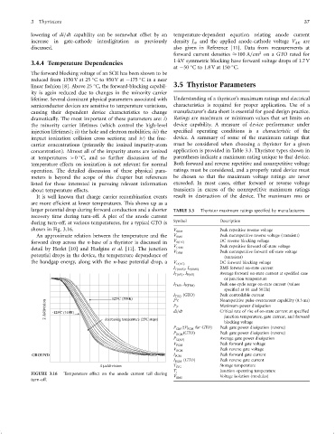
It is well known that charge carrier recombination events result in destruction of the device. The maximum rms or
are more ef®cient at lower temperatures. This shows up as a
larger potential drop during forward conduction and a shorter TABLE 3.3 Thyristor maximum ratings speci®ed by manufacturers
recovery time during turn-off. A plot of the anode current
during turn-off, at various temperatures, for a typical GTO is Symbol Description
shown in Fig. 3.16. V RRM Peak repetitive reverse voltage
An approximate relation between the temperature and the V RMS Peak nonrepetitive reverse voltage (transient)
forward drop across the n-base of a thyristor is discussed in V RðDCÞ DC reverse blocking voltage
Peak repetitive forward off-state voltage
detail by Herlet [10] and Hudgins et al. [11]. The junction
V DRM
V DSM Peak nonrepetitive forward off-state voltage
potential drops in the device, the temperature dependence of (transient)
the bandgap energy, along with the n-base potential drop, a V DðDCÞ DC forward blocking voltage
RMS forward on-state current
I TðRMSÞ , I FðRMSÞ
Average forward on-state current at speci®ed case
I TðAVÞ , I FðAVÞ
or junction temperature
Peak one-cycle surge on-state current (values
I TMS , I FðTSMÞ
speci®ed at 60 and 50 Hz)
I TGQ (GTO) Peak controllable current
125 o C (398K) I t Nonrepetitive pulse overcurrent capability (8.3 ms)
2
2 A/division -125 o C (148K) P T Maximum power dissipation
Critical rate of rise of on-state current at speci®ed
di=dt
junction temperature, gate current, and forward
decreasing temperature (25 o C steps)
blocking voltage
P GM =ðP FGM for GTO) Peak gate power dissipation (reverse)
P RGM ðGTOÞ Peak gate power dissipation (reverse)
Average gate power dissipation
P GðAVÞ
Peak forward gate voltage
V FGM
Peak reverse gate voltage
V RGM
GROUND I FGM Peak forward gate current
I RGM (GTO) Peak reverse gate current
4 m s/division T STG Storage temperature
Junction operating temperature
T j
FIGURE 3.16 Temperature effect on the anode current tail during
V RMS Voltage isolation (modules)
turn-off.