
Page 53 - Rashid, Power Electronics Handbook
P. 53
J. Hudgins et al.
3838 J. Hudgins et al.
average current ratings given are usually those that cause the TABLE 3.4 Typical thyristor characteristic maximums and minimum
junction to reach its maximum rated temperature. Because the speci®ed by manufacturers
maximum current will depend upon the current waveform
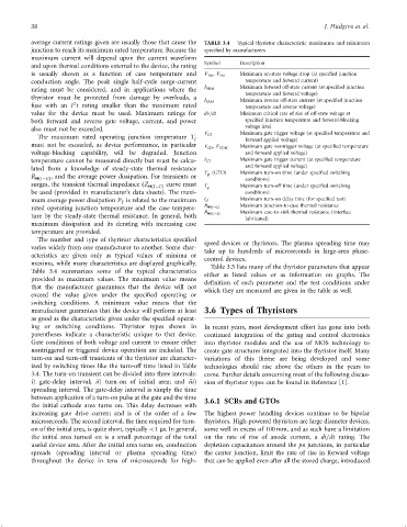
Symbol Description
and upon thermal conditions external to the device, the rating
is usually shown as a function of case temperature and V TM , V FM Maximum on-state voltage drop (at speci®ed junction
conduction angle. The peak single half-cycle surge-current temperature and forward current)
Maximum forward off-state current (at speci®ed junction
I DRM
rating must be considered, and in applications where the
temperature and forward voltage)
thyristor must be protected from damage by overloads, a
I RRM Maximum reverse off-state current (at speci®ed junction
2
fuse with an I t rating smaller than the maximum rated temperature and reverse voltage)
value for the device must be used. Maximum ratings for dn=dt Minimum critical rate of rise of off-state voltage at
both forward and reverse gate voltage, current, and power speci®ed junction temperature and forward-blocking
voltage level
also must not be exceeded. Maximum gate trigger voltage (at speci®ed temperature and
The maximum rated operating junction temperature T V GT
J forward applied voltage)
must not be exceeded, as device performance, in particular Maximum gate nontrigger voltage (at speci®ed temperature
V GD , V GDM
voltage-blocking capability, will be degraded. Junction and forward applied voltage)
temperature cannot be measured directly but must be calcu- I GT Maximum gate trigger current (at speci®ed temperature
lated from a knowledge of steady-state thermal resistance and forward applied voltage)
T gt (GTO) Maximum turn-on time (under speci®ed switching
R YðJÿCÞ , and the average power dissipation. For transients or conditions)
surges, the transient thermal impedance ðZ YðJÿCÞ curve must T q Maximum turn-off time (under speci®ed switching
be used (provided in manufacturer's data sheets). The maxi- conditions)
mum average power dissipation P is related to the maximum t D Maximum turn-on delay time (for speci®ed test)
T
rated operating junction temperature and the case tempera- R YðJÿCÞ Maximum junction-to-case thermal resistance
Maximum case-to-sink thermal resistance (interface
R YðCÿSÞ
ture by the steady-state thermal resistance. In general, both
lubricated)
maximum dissipation and its derating with increasing case
temperature are provided.
The number and type of thyristor characteristics speci®ed
speed devices or thyristors. The plasma spreading time may
varies widely from one manufacturer to another. Some char-
take up to hundreds of microseconds in large-area phase-
acteristics are given only as typical values of minima or
control devices.
maxima, while many characteristics are displayed graphically.
Table 3.5 lists many of the thyristor parameters that appear
Table 3.4 summarizes some of the typical characteristics either as listed values or as information on graphs. The
provided as maximum values. The maximum value means de®nition of each parameter and the test conditions under
that the manufacturer guarantees that the device will not which they are measured are given in the table as well.
exceed the value given under the speci®ed operating or
switching conditions. A minimum value means that the
manufacturer guarantees that the device will perform at least 3.6 Types of Thyristors
as good as the characteristic given under the speci®ed operat-
ing or switching conditions. Thyristor types shown in In recent years, most development effort has gone into both
parentheses indicate a characteristic unique to that device. continued integration of the gating and control electronics
Gate conditions of both voltage and current to ensure either into thyristor modules and the use of MOS technology to
nontriggered or triggered device operation are included. The create gate structures integrated into the thyristor itself. Many
turn-on and turn-off transients of the thyristor are character- variations of this theme are being developed and some
ized by switching times like the turn-off time listed in Table technologies should rise above the others in the years to
3.4. The turn-on transient can be divided into three intervals: come. Further details concerning most of the following discus-
i) gate-delay interval; ii) turn-on of initial area; and iii) sion of thyristor types can be found in Reference [1].
spreading interval. The gate-delay interval is simply the time
between application of a turn-on pulse at the gate and the time 3.6.1 SCRs and GTOs
the initial cathode area turns on. This delay decreases with
increasing gate drive current and is of the order of a few The highest power handling devices continue to be bipolar
microseconds. The second interval, the time required for turn- thyristors. High-powered thyristors are large diameter devices,
on of the initial area, is quite short, typically <1 ms. In general, some well in excess of 100 mm, and as such have a limitation
the initial area turned on is a small percentage of the total on the rate of rise of anode current, a di=dt rating. The
useful device area. After the initial area turns on, conduction depletion capacitances around the pn junctions, in particular
spreads (spreading interval or plasma spreading time) the center junction, limit the rate of rise in forward voltage
throughout the device in tens of microseconds for high- that can be applied even after all the stored charge, introduced