
Page 46 - Rashid, Power Electronics Handbook
P. 46
3 Thyristors 31
latching current I . If the thyristor is already in forward-
L
conduction and the anode current is reduced, the device can
move its operating mode from forward-conduction back to
forward-blocking. The minimum value of anode current
necessary to keep the device in forward-conduction after it
has been operating at a high anode current value is called the
holding current I . The holding current value is lower than
H
the latching current value as indicated in Fig. 3.3.
The reverse thyristor characteristic, quadrant III of Fig. 3.3,
is determined by the outer two junctions (J and J ), which are
1 3
reverse-biased in this operating mode (applied n is nega-
AK
tive). Symmetric thyristors are designed so that J will reach
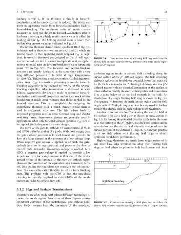
1 FIGURE 3.4 Cross section showing a ¯oating ®eld ring to decrease the
reverse breakdown due to carrier multiplication at an applied electric ®eld intensity near the curved portion of the main anode region
reverse potential near the forward breakdown value (operating (leftmost p -region).
þ
point ‘‘3'' in Fig. 3.3). The forward- and reverse-blocking
junctions are usually fabricated at the same time with a very
depletion region results in electric ®eld crowding along the
long diffusion process (10 to 50 h) at high temperatures þ
(>1200 C). This process produces symmetric blocking prop- curved section of the p -diffused region. The ®eld crowding
seriously reduces the breakdown potential below that expected
erties. Wafer-edge termination processing causes the forward- þ
for the bulk semiconductor. A ¯oating ®eld ring, an extra p -
blocking capability to be reduced to 90% of the reverse- diffused region with no electrical connection at the surface, is
blocking capability. Edge termination is discussed in what
often added to modify the electric ®eld pro®le and thus reduce
follows. Asymmetric devices are made to optimize forward-
it to a value below or at the ®eld strength in the bulk. An
conduction and turn-off properties, and as such reach reverse
illustration of a single ¯oating ®eld ring is shown in Fig. 3.4.
breakdown at much lower voltages than those applied in the
The spacing W between the main anode region and the ®eld
forward direction. This is accomplished by designing the
ring is critical. Multiple rings can also be employed to further
asymmetric thyristor with a much thinner n-base than is
modify the electric ®eld in high-voltage rated thyristors.
used in symmetric structures. The thin n-base leads to
Another common method for altering the electric ®eld at
improved properties such as lower forward drop and shorter
the surface is to use a ®eld plate as shown in cross section in
switching times. Asymmetric devices are generally used in
applications when only forward voltages (positive n AK ) are to Fig. 3.5. By forcing the potential over the oxide to be the same
þ
be applied (including many inverter designs). as at the surface of the p -region, the depletion region can be
The form of the gate-to-cathode VI characteristic of SCRs extended so that the electric ®eld intensity is reduced near the
þ
and GTOs is similar to that of a diode. With positive gate bias, curved portion of the diffused p -region. A common practice
is to use ®eld plates with ¯oating ®eld rings to obtain
the gate-cathode junction is forward-biased and permits the
optimum breakdown performance.
¯ow of a large current in the presence of a low voltage drop.
High-voltage thyristors are made from single wafers of Si
When negative gate voltage is applied to an SCR, the gate-
and must have edge terminations other than ¯oating ®eld
cathode junction is reverse-biased and prevents the ¯ow of
rings or ®eld plates to promote bulk breakdown and limit
current until avalanche breakdown voltage is reached. In a
GTO, a negative gate voltage is applied to provide a low
impedance path for anode current to ¯ow out of the device
instead of out of the cathode. In this way the cathode region
(base-emitter junction of the equivalent npn transistor) turns
off, thus pulling the equivalent npn transistor out of conduc-
tion. This causes the entire thyristor to return to its blocking
state. The problem with the GTO is that the gate-drive
circuitry is typically required to sink 10% of the anode
current in order to achieve turn-off.
3.3.2 Edge and Surface Terminations
Thyristors are often made with planar diffusion technology to
create the anode region. Formation of these regions creates
cylindrical curvature of the metallurgical gate-cathode junc- FIGURE 3.5 Cross section showing a ®eld plate used to reduce the
tion. Under reverse bias, the curvature of the associated electric ®eld intensity near the curved portion of the p -region (anode).
þ