
Page 85 - Renewable Energy Devices and System with Simulations in MATLAB and ANSYS
P. 85
72 Renewable Energy Devices and Systems with Simulations in MATLAB and ANSYS ®
®
achieved, while high efficiency is still maintained. Besides the higher costs of the SiC and GaN, new
challenges need to be dealt with, like radiated and conducted EMI [31].
The drive for higher efficiencies has led to the use of multilevel topologies like neutral point
clamped (NPC) [32] or T type [33], also sketched in Figure 4.3, resulting in a decrease in filter
requirements and increase in the overall efficiency of the system, thanks to the multilevel output
voltage. Some of these multilevel topologies are also preferred in high power applications, due to the
reduced voltage stress of the power devices, compared to a traditional two-level converter. Several
companies use these multilevel topologies in their MCIs within a range of 10–60 kW and these
MCIs are being used in MW-sized PV plants, where the modularity given by this topology is a huge
advantage during installation, operation, and maintenance.
In order to maintain high efficiency over a wide range of power levels and to ensure fault-tolerant
operation for the converter, a new trend is to apply modular topologies, such as modular multilevel
converters (MMC) or paralleled converters. The MMC consist of series-connected cells, usually
with half- or full-bridge topology [34]. The number of cells used in a phase of the MMC will define
the discrete voltage levels at the output of the converter; thus, the size of the passive filters between
the MMC and grid can be reduced considerably. Another advantage of such topology is the pos-
sibility of using LV power switches. By adding redundant cells on each phase of the converter,
fault-tolerant operation can be ensured [35]. By paralleling inverters, a flat efficiency profile can be
achieved over a wide power range, where the number of parallel-connected inverters depends on the
available power from the solar panels [36]. The parallel configuration for the central inverter ensures
also fault-tolerant operation. By using interleaving between the modulation carrier wave, the current
THD can be reduced considerably [37].
4.4 CONTROL BUILDING BLOCKS FOR PV INVERTERS
4.4.1 Modulation Strategies for Three-Phase PV Inverters
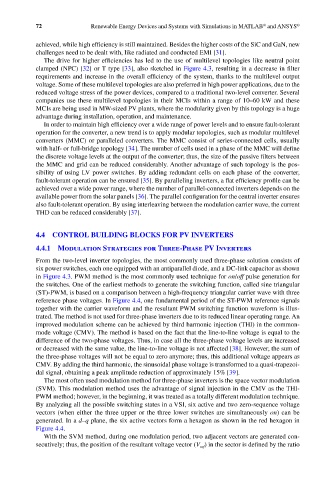
From the two-level inverter topologies, the most commonly used three-phase solution consists of
six power switches, each one equipped with an antiparallel diode, and a DC-link capacitor as shown
in Figure 4.3. PWM method is the most commonly used technique for on/off pulse generation for
the switches. One of the earliest methods to generate the switching function, called sine triangular
(ST)-PWM, is based on a comparison between a high-frequency triangular carrier wave with three
reference phase voltages. In Figure 4.4, one fundamental period of the ST-PWM reference signals
together with the carrier waveform and the resultant PWM switching function waveform is illus-
trated. The method is not used for three-phase inverters due to its reduced linear operating range. An
improved modulation scheme can be achieved by third harmonic injection (THI) in the common-
mode voltage (CMV). The method is based on the fact that the line-to-line voltage is equal to the
difference of the two-phase voltages. Thus, in case all the three-phase voltage levels are increased
or decreased with the same value, the line-to-line voltage is not affected [38]. However, the sum of
the three-phase voltages will not be equal to zero anymore; thus, this additional voltage appears as
CMV. By adding the third harmonic, the sinusoidal phase voltage is transformed to a quasi-trapezoi-
dal signal, obtaining a peak amplitude reduction of approximately 15% [39].
The most often used modulation method for three-phase inverters is the space vector modulation
(SVM). This modulation method uses the advantage of signal injection in the CMV as the THI-
PWM method; however, in the beginning, it was treated as a totally different modulation technique.
By analyzing all the possible switching states in a VSI, six active and two zero-sequence voltage
vectors (when either the three upper or the three lower switches are simultaneously on) can be
generated. In a d–q plane, the six active vectors form a hexagon as shown in the red hexagon in
Figure 4.4.
With the SVM method, during one modulation period, two adjacent vectors are generated con-
secutively; thus, the position of the resultant voltage vector (V ) in the sector is defined by the ratio
ref