
Page 86 - Renewable Energy Devices and System with Simulations in MATLAB and ANSYS
P. 86
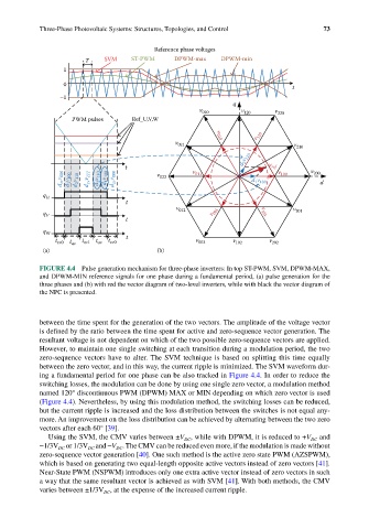
Three-Phase Photovoltaic Systems: Structures, Topologies, and Control        73


                                           Reference phase voltages
                        T    SVM     ST-PWM      DPWM-max    DPWM-min
                  1

                  0
                                                                                 t
                 –1
                                                                 q
                                                       v 020       v 120    v 220
                     PWM pulses      Ref_U,V,W
                                                                       v 110
                                                            v 010
                                                 v 021                           v 210
                                                                   d 2 v 110
                                   t                  v                   v ref  v    v
                  d zv v 000  d 1 v 100  d 2 v 110  d zv v 111  d 2 v 110  d 1 v 100  d zv v 000  v 022  011  d 1 v 100  100  200 d


             q U
                                   t
                                                 v 012                           v 201
             q V                                           v 001        v 101
                                   t
             q W
                t zv0  t av  t zv1 t av  t zv0  t     v 002      v 102    v 202
             (a)                            (b)

            FIGURE 4.4  Pulse generation mechanism for three-phase inverters: In top ST-PWM, SVM, DPWM-MAX,
            and DPWM-MIN reference signals for one phase during a fundamental period, (a) pulse generation for the
            three phases and (b) with red the vector diagram of two-level inverters, while with black the vector diagram of
            the NPC is presented.


            between the time spent for the generation of the two vectors. The amplitude of the voltage vector
            is defined by the ratio between the time spent for active and zero-sequence vector generation. The
            resultant voltage is not dependent on which of the two possible zero-sequence vectors are applied.
            However, to maintain one single switching at each transition during a modulation period, the two
            zero-sequence vectors have to alter. The SVM technique is based on splitting this time equally
            between the zero vector, and in this way, the current ripple is minimized. The SVM waveform dur-
            ing a fundamental period for one phase can be also tracked in Figure 4.4. In order to reduce the
            switching losses, the modulation can be done by using one single zero vector, a modulation method
            named 120° discontinuous PWM (DPWM) MAX or MIN depending on which zero vector is used
            (Figure 4.4). Nevertheless, by using this modulation method, the switching losses can be reduced,
            but the current ripple is increased and the loss distribution between the switches is not equal any-
            more. An improvement on the loss distribution can be achieved by alternating between the two zero
            vectors after each 60° [39].
              Using the SVM, the CMV varies between ±V , while with DPWM, it is reduced to +V  and
                                                                                      DC
                                                   DC
            −1/3V  or 1/3V  and −V . The CMV can be reduced even more, if the modulation is made without
                         DC
                 DC
                                 DC
            zero-sequence vector generation [40]. One such method is the active zero state PWM (AZSPWM),
            which is based on generating two equal-length opposite active vectors instead of zero vectors [41].
            Near-State PWM (NSPWM) introduces only one extra active vector instead of zero vectors in such
            a way that the same resultant vector is achieved as with SVM [41]. With both methods, the CMV
            varies between ±1/3V , at the expense of the increased current ripple.
                             DC