Page 88 - Renewable Energy Devices and System with Simulations in MATLAB and ANSYS
P. 88

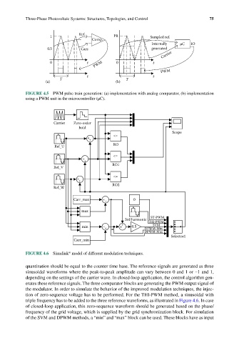
Three-Phase Photovoltaic Systems: Structures, Topologies, and Control        75


                                  Ref.
                      1                          PR             Sampled ref.
                                        Comp.
                                                                 Internally  µC  IO
                     0.5           Carr.                         generated
                                                                     Carrier

                                         PWM
                      0               t           0              t
                                                                     PWM
                                      t                          t
                          T                           T
                    (a)                           (b)

            FIGURE 4.5  PWM pulse train generation: (a) implementation with analog comparator, (b) implementation
            using a PWM unit in the microcontroller (μC).


                        Carrier  Zero-order
                                  hold
                                                                          Scope
                                                 <=
                                      + +
                        Ref_U                    RO
                                                 <=
                                    + +
                                                RO1
                        Ref_V

                                                 <=
                                 + +
                                                RO2
                        Ref_W

                                Carr_max    + –          0

                                   max
                                                                ST-PWM
                                                      3rd harmonic  THI-PWM
                                                                 SVM
                                   min      – +    + +  0.5   DPWM-Min
                                                              DPWM-Max
                                                                         Selector1
                                Carr_min


                              ®
            FIGURE 4.6  Simulink  model of different modulation techniques.
            quantization should be equal to the counter time base. The reference signals are generated as three
            sinusoidal waveforms where the peak-to-peak amplitude can vary between 0 and 1 or −1 and 1,
            depending on the settings of the carrier wave. In closed-loop application, the control algorithm gen-
            erates these reference signals. The three comparator blocks are generating the PWM output signal of
            the modulator. In order to simulate the behavior of the improved modulation techniques, the injec-
            tion of zero-sequence voltage has to be performed. For the THI-PWM method, a sinusoidal with
            triple frequency has to be added to the three reference waveforms, as illustrated in Figure 4.6. In case
            of closed-loop application, this zero-sequence waveform should be generated based on the phase/
            frequency of the grid voltage, which is supplied by the grid synchronization block. For simulation
            of the SVM and DPWM methods, a “min” and “max” block can be used. These blocks have as input
   83   84   85   86   87   88   89   90   91   92   93