
Page 87 - Renewable Energy Devices and System with Simulations in MATLAB and ANSYS
P. 87
74 Renewable Energy Devices and Systems with Simulations in MATLAB and ANSYS ®
®
The spectrum of the output voltage of each modulation technique can be determined by analytical
equations, which can be used for efficiency calculations [38, 42]. By using different random modu-
lation techniques, the discrete components from the output voltage spectrum can be spread, which
can improve the electromagnetic compatibility (EMC) of the converter [43].
From the modulation techniques mentioned earlier, SVM is the most commonly used method due
to its lowest current ripple. However, in high power applications, where the switching loss reduction
is important due to the complex thermal management, DPWM or a modified version of it is pre-
ferred. The reduction of the peak-to-peak CMV is important in PV applications; thus, the AZSPWM
or NSPWM methods can be a good alternative.
For high-power inverters, the NPC topology is often used. The topology is based on using two
capacitors placed in series in the DC link, with the midpoint connected to the inverter neutral point,
as shown in Figure 4.3. The voltage balancing of the two capacitors is an essential task for NPC
topologies; the modulation has to have the ability to ensure this balance. From an implementation
point of view, there are two approaches: carrier based (CB) [44] and SVM [45]. The CB meth-
ods are the phase disposition (PD-PWM), phase opposition disposition (POD-PWM), and alter-
nate phase opposition (APOD-PWM). The difference between the CB methods is the phase shift
between the carrier waves. In the PD method, both the positive and negative carriers are in phase,
while in POD the carriers for the positive references are 180° shifted from the negative reference
carriers. For the APOD method, the two carrier waves are for both positive and negative part of
the reference voltage and they are 180° phase shifted from each other. From the three methods,
PD-PWM has the lowest harmonic distortion, while APOD and POD PWM strategies are similar
[44]. The SVM technique for NPC is implemented similarly as for two-level topologies shown in
Figure 4.4 and uses the freedom given by the zero-sequence vector redistribution; thus, it can be
easily optimized for low switching loss [46].
4.4.2 Implementation of the Modulation Strategies
The implementation of the modulation strategies can be achieved by using analog or digital compo-
nents. For the analog implementation, a carrier wave generator and an analog comparator are needed
between the carrier waveform and the reference signal, as it is sketched in Figure 4.4. Today, such
an implementation method is rarely used because it is not flexible. In most applications, the overall
system control implemented in microcontrollers is straightforward by using digitally implemented
modulators. Moreover, the microcontrollers are usually equipped with a dedicated PWM unit. The
PWM unit consists of a counter, which generates the carrier wave and a compare register (CR),
where the reference signal is loaded at each sampling period. The counter is reset or changed from
up-count mode to down-count mode (depending on whether sawtooth or triangular carrier needs to
be generated) when it reaches the value loaded in the period register (PR). Thus, through the PR, the
frequency of the carrier wave is established. The new values for the CR are usually loaded when the
counter takes the value of zero and/or the value of PR as shown in Figure 4.5. At the time instance,
when the counter reaches the CR value, the input/output port (which has to be set as output port) of
the microcontroller performs the switching.
®
®
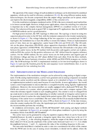
In simulation environments, such as MATLAB /Simulink , both analog and digital methods
are easy to implement. In Figure 4.6, an example of a three-phase modulator is given by using the
elementary blocks from MATLAB /Simulink .
®
®
The carrier wave can be generated by using the repetitive sequence block (it can be found under
Simulink/Sources). In order to generate a triangular signal, three time values have to be set [1 1/
(2F ) 1/F ] where F is the switching frequency, while the output of the block should also take
sw
sw
sw
three values [0 1 0] in case the amplitude of the carrier varies between 0 and 1 or [−1 1–1] to obtain
the amplitude between −1 and 1. F represents the value of the switching frequency in this case.
sw
The zero-order hold block is inserted in order to take into consideration the effect of the counter
from the PWM unit (in the case of analog circuit simulation, it should not be added), where the