
Page 138 - Semiconductor Manufacturing Handbook
P. 138
Geng(SMH)_CH10.qxd 04/04/2005 19:46 Page 10.11
ION IMPLANTATION AND RAPID THERMAL PROCESSING
ION IMPLANTATION AND RAPID THERMAL PROCESSING 10.11
The uniformity of delivered ion dose across a wafer in modern ion implantation tools is typically
expected to have a standard deviation no greater than approximately 0.5 percent, as measured with
the most sensitive means available.
Thermal Annealing and Junction Formation. Postimplant thermal annealing is required to repair
the crystalline structure of the wafer from the damage created during implantation and to provide for
some level of electrical activation of the newly introduced dopant ions. Various techniques for per-
forming the annealing step are available, but can be broadly grouped according to whether they are
more isothermal or adiabatic in nature. Adiabatic processes must take place on time scales of the
order of microseconds or shorter, and are not common in mainstream high-volume manufacturing
today. Isothermal annealing, with time scales ranging from hundreds of milliseconds to minutes is
20
dominant and can be achieved with a variety of types of equipment. Most common for isothermal
advanced anneal processing today are still lamp-based or hot-walled furnaces. The former typically
uses arrays of high-power filament lamps arranged and controlled to provide uniform radiation over
one or both surfaces of the wafer. The latter establishes a controlled spatial temperature profile within
a volume and then positions the wafer within that volume to achieve the desired temperature and
time profile for the process. Both can be used in regimes that range from more conventional long
anneal times to rapid thermal anneals (RTA). As trends toward ultrashallow junction formation call
for ever-decreasing thermal budgets for the wafer to minimize dopant diffusion, their abilities to
serve as robust RTA tools is increasingly challenged.
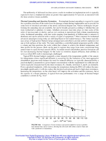
Typical RTA thermal budgets (generally a time integral of the temperature profile of the anneal,
for temperatures where significant diffusion is occurring) for the formation of the most aggressive
ultrashallow junctions must balance the need for reduced diffusion (as typically characterized by a
junction depth X measured at a given dopant concentration) with the requirement for sufficient acti-
j
vation (typically characterized by the sheet resistance R ). Ideally, minimum X and R are desirable.
s j s
From a practical standpoint, while decreasing the temperature during the RTA will reduce the junc-
tion depth significantly, it will also reduce the electrical activation and lead to high sheet resistances.
Increasing the temperature, on the other hand, will improve the activation and the resistance, but at
the expense of a deeper junction. A typical best-case performance over a range of thermal budget
conditions is shown in Fig. 10.6. 6
1000
-
-
R d (Ohm/sq)
100
0 10 20 30 40 50 60 70 80 90 100 110 120
18
−3
x at 1 × 10 cm (nm)
j
FIGURE 10.6 Comparison of sheet resistance and junction depth for various rapid ther-
mal anneals from various sources, showing that all results fall within a narrow band and
with a predicted 1/x dependence.
Downloaded from Digital Engineering Library @ McGraw-Hill (www.digitalengineeringlibrary.com)
Copyright © 2004 The McGraw-Hill Companies. All rights reserved.
Any use is subject to the Terms of Use as given at the website.