
Page 141 - Semiconductor Manufacturing Handbook
P. 141
Geng(SMH)_CH10.qxd 04/04/2005 19:46 Page 10.14
ION IMPLANTATION AND RAPID THERMAL PROCESSING
10.14 WAFER PROCESSING
these “mass coincidences” include Mo ++ and BF (both have an apparent mass of 49 amu).
2
Molybdenum is a common ion source arc chamber material that ionizes relatively easily; it is not
uncommon for this energetic contaminant to have levels as high as several tenths of a percent.
Manufacturers who rely on BF implants often turn to more expensive tungsten arc chambers specif-
2
+
+
ically to avoid this issue. Other common energetic contaminants include PF in BF (masses 50 and
2
+
49, respectively) but are only present following long periods of P operation and can be easily miti-
gated with simple in situ plasma cleaning steps during process recipe transitions from one species to
another.
10.4.4 Wafer Charge Control
Delivering a large number of ions to the wafer can lead to very high electrostatic potentials if there
28
is not a sufficient supply of electrons to neutralize the positive charge as it arrives. Beam poten-
tials (and hence wafer potentials) of tens or even hundreds of volts would be commonplace with-
out such a supply of electrons. Of greatest concern in the face of such potentials is the integrity of
the dielectric gate oxide. Despite the fact that high-quality gate oxides can have breakdown fields
as high as 10 to 15 MV/cm, the gate oxides in modern devices are now no more than a few atoms
thick and are susceptible to breakdown with applied voltages of no more than a few volts. Luckily,
significant neutralization of these high potentials is achieved using electrons from a number of
sources. Secondary electrons generated by ion beam impact with the wafer itself and its support-
ing structures play a role in helping to control wafer charging. All modern high-current tools also
have active plasma sources in the vicinity of the wafer to provide an additional supply of electrons
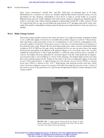
to aid in this neutralization. A typical design for such plasma electron floods (PEFs) or plasma
flood guns (PFGs) is shown in Fig. 10.8. 29 High-energy and medium-current tools have either
active electron or plasma sources or a means of locally increasing the pressure in the vicinity of
the wafer to assist in the generation of a significant enough plasma beam to ensure adequate wafer
charge control.
FIGURE 10.8 A typical plasma electron flood gun design for high-
current architectures. The PEF sits just before the wafer. The ion beam
is incident from right to left in this drawing.
Downloaded from Digital Engineering Library @ McGraw-Hill (www.digitalengineeringlibrary.com)
Copyright © 2004 The McGraw-Hill Companies. All rights reserved.
Any use is subject to the Terms of Use as given at the website.