
Page 140 - Semiconductor Manufacturing Handbook
P. 140
Geng(SMH)_CH10.qxd 04/04/2005 19:46 Page 10.13
ION IMPLANTATION AND RAPID THERMAL PROCESSING
ION IMPLANTATION AND RAPID THERMAL PROCESSING 10.13
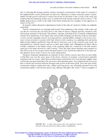
risk of collecting this foreign material. Surface elemental contamination of the order of 1 percent of
the implanted dose can be problematic for processes. Measures to reduce elemental surface contam-
ination include general reduction of surface area struck by the beam in the vicinity of the wafer and
25
ensuring that the remaining surface area is coated with more benign materials such as silicon. The
highly spoked process disks in the multi-wafer batch architecture are examples of this approach, as
shown in Fig 10.7.
In general, surface elemental contamination levels of the order of 1 percent or better are routinely
achievable.
Particle contamination can originate both locally from sputtering in the vicinity of the wafer and
can also be carried by the ion beam itself, in the form of massive charged particles entrained in the
electrostatic potential of the beam. The primary concerns with high levels of particle contamination
include local shadowing of the dopant dose and possible bridging and shorting of device structures.
A more recently emerging concern involving particles causing ballistic damage to fine device struc-
tures is more prevalent in systems with high-velocity wafer scanning via a spinning disk and during
high-current implants performed when tall device structures such as the transistor gate stacks are
unsupported by sidewall spacers and are in their most fragile state. Mitigations for these effects
include a reduction of the kinetic energy in the scanning wafers by a reduction of the disk rotation
26
speed up to the limits allowed by wafer cooling. Since the high-current implants most sensitive to
this effect occur at low energies where the beam power is low, significant reductions in the disk rota-
tion speed (a factor of ten or more) are easily implemented.
Energetic elemental contaminants are typically of more serious concern, since they are more likely
to find their way into the active areas of the device. Sources of energetic contamination generally
originate at the ion source, either from residual dopant material left over from previous implant steps
or from the structural materials of the ion source and extraction optics. Any material in the ion source
that is ionized and extracted will pass through some portion of the beam guide. Since the mass (really
momentum) analysis magnet has only a finite resolving power, any unwanted extracted ions with
27
momentum similar to the desired species may still pass through to the wafer. Classic examples of
FIGURE 10.7 A multi-wafer process disk with significant material
between wafer pads removed to reduce surface contamination.
Downloaded from Digital Engineering Library @ McGraw-Hill (www.digitalengineeringlibrary.com)
Copyright © 2004 The McGraw-Hill Companies. All rights reserved.
Any use is subject to the Terms of Use as given at the website.