
Page 241 - Semiconductor Manufacturing Handbook
P. 241
Geng(SMH)_CH16.qxd 04/04/2005 19:54 Page 16.8
ECD FUNDAMENTALS
16.8 WAFER PROCESSING
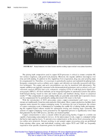
FIGURE 16.7 Bump formation over dense features and the resulting copper residual versus planar deposition.
The plating bath composition used in copper ECD processes is critical to ensure complete fill,
low surface roughness, and good local planarity. However, the organic additives decompose over
time and with plating. In addition to this, liquid loss from evaporation, drag out, and sampling must
be compensated for. Therefore, it is necessary to periodically analyze and replenish the plating bath.
Inorganic components such as sulfuric acid, copper, and chlorides are typically measured with titra-
tion techniques. The copper and acid concentrations can also be measured with photometry. The
organic additives are typically measured with electroanalytical techniques such as pulsed cyclic gal-
vanostatic analysis (PCGA) and cyclic voltametric stripping (CVS) or with high purity liquid chro-
motography (HPLC). All these methods can be integrated together in automated systems that utilize
feed-forward dosing, based on time and wafers plated, and feedback dosing, based on analytical
results. 18,37 The components of copper plating baths are generally nonvolatile and evaporative losses
can be compensated for by periodically adding deionized (DI) water to the bath.
With the introduction of ECD processing comes copper-contaminated acid waste—a waste
stream not traditionally found in semiconductor fabrication. Most copper production facilities have
separate waste streams for copper-containing waste. To minimize the cost of treatment, the volume
of copper-containing waste is minimized by extending the usable life of plating baths and minimiz-
ing the required liquid volume needed for subsequent rinsing and cleaning steps. Generally, the
amount of copper-containing waste generated by the deposition process is significantly lower than
that generated by the CMP process, and they are treated together.
Copper contamination is also a concern within the processing facility. Copper is a mobile ion
capable of poisoning semiconductor devices. At the interconnect levels, copper is contained within
the barrier and capping layers. To prevent cross contamination at the device level, processing facili-
ties utilize strict protocols. Persons working in and around copper processing areas are prohibited
from entering other areas, and individuals working with copper ECD and CMP are frequently
required to wear specific cleanroom gowns for identification.
Downloaded from Digital Engineering Library @ McGraw-Hill (www.digitalengineeringlibrary.com)
Copyright © 2004 The McGraw-Hill Companies. All rights reserved.
Any use is subject to the Terms of Use as given at the website.