
Page 239 - Semiconductor Manufacturing Handbook
P. 239
Geng(SMH)_CH16.qxd 04/04/2005 19:54 Page 16.6
ECD FUNDAMENTALS
16.6 WAFER PROCESSING
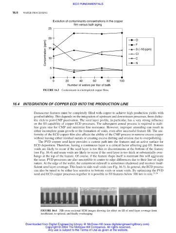
Evolution of contaminants concentrations in the copper
film versus bath aging
25
20 O
Concentration (ppm) 15 S (×10 ppm)
F
Cl
10
C
5 N
0
0 20 40 60 80 100
Number of wafers per liter of bath
FIGURE 16.3 Contaminants in electroplated copper films.
16.4 INTEGRATION OF COPPER ECD INTO THE PRODUCTION LINE
Damascene features must be completely filled with copper to achieve high production yields with
good reliability. This depends on the integration of upstream and downstream processes, from dielec-
tric etch to post-CMP passivation. The seed layer profile, in particular, has a very strong influence
on the fill capability of copper ECD processes. The subsequent anneal process is required to stabi-
lize grain size for CMP and minimize line resistance. However, improper annealing can result in
either incomplete grain growth or the formation of voids, even after successful feature fill. The uni-
formity of the ECD copper film also affects the ability of the CMP process to remove excess copper
without leaving either residual metals or creating excess dishing and erosion due to overpolishing.
The PVD copper seed layer provides a current path into the features and an active surface for
ECD deposition. Therefore, having a continuous layer is a critical factor affecting gap fill. Bottom
voids are likely to occur if the seed layer is too thin or discontinuous at the bottom of the feature
(see Fig. 16.4) and seam voids are likely to occur if the seed layer is too thick or substantially over-
hangs at the top of the feature. Of course, if the feature shape itself is reentrant this will aggravate
the issue. PVD processes are also susceptible to center-to-edge differences due to their line-of-sight
nature. At the edge of the wafer, the centermost sidewall is sometimes shadowed and receives insuf-
ficient seed layer coverage. This leads to side-wall voids (see Fig. 16.5). In general, the ECD process
can also be tuned to be either less sensitive to bottom voids or seam voids. By optimizing the PVD
seed and ECD copper processes together it is possible to fill features below 100 nm in size. 23,24
FIGURE 16.4 FIB cross-sectional SEM images showing the effect on fill of seed layer coverage from
insufficient, to optimal, and finally overhanging.
Downloaded from Digital Engineering Library @ McGraw-Hill (www.digitalengineeringlibrary.com)
Copyright © 2004 The McGraw-Hill Companies. All rights reserved.
Any use is subject to the Terms of Use as given at the website.