
Page 242 - Semiconductor Manufacturing Handbook
P. 242
Geng(SMH)_CH16.qxd 04/04/2005 19:54 Page 16.9
ECD FUNDAMENTALS
ECD FUNDAMENTALS 16.9
16.6 FUTURE TRENDS
With each technology node, interconnect size decreases and the current density in interconnects
increases. (According to the International Technology Roadmap for Semiconductors, the current den-
38
sity will approximately double from the 130-nm to the 45-nm node technology. ) This translates to
higher line resistance and increased susceptibility to electromigration. Semiconductor companies are
actively pursuing techniques to manage both of these factors.
As feature sizes become smaller, the percentage of the interconnect filled by the barrier layer
becomes more significant. In addition to this, the size of the interconnect feature is approaching the
electron mean-free path in copper, causing the resistivity to increase due to surface scattering of elec-
trons. To minimize line resistance, barrier layers must become thinner, smoother, and more conduc-
tive, while continuing to prevent diffusion of copper atoms into the dielectric material. The minimal
barrier thickness is determined by the conformality of the deposit. For this reason, atomic layer
deposition (ALD)—a derivative of CVD technology—looks very promising. ALD processes deposit
barrier materials with nearly 100 percent conformality. Chip manufacturers are also investigating
higher-conductivity barrier materials including ruthenium and tungsten.
Current process technology utilizes either a blanket layer of silicon nitride or silicon carbide (or
a combination) to cap the copper lines after CMP. This insulating layer provides sufficient protec-
tion against copper diffusion and serves as an etch stop. However, electromigration occurs primarily
39
along this interface, reducing the device lifetime. This layer also has a relatively high dielectric
constant, which increases the effective dielectric constant of the dielectric stack. To achieve effective
dielectric constants significantly below 3.0, the blanket-capping layer must be either changed or
eliminated. 40
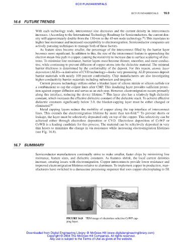
Metal capping layers reduce the mobility of copper along the top interface of interconnect
lines. This extends the electromigration lifetime by more than ten-fold. 41 To prevent shorts or
leakage, the layer must be selectively deposited only on top of the copper. This selectivity can be
achieved either through electroless deposition or CVD. Electroless deposition of CoWP or
CoWB is a leading candidate for this process. The material can be selectively deposited in very
thin layers to minimize the change in via resistance while increasing electromigration lifetimes
(see Fig. 16.8).
16.7 SUMMARY
Semiconductor manufacturers continually strive to make smaller, faster chips by minimizing line
resistance, feature sizes, and dielectric constants. As features shrink, the local current densities
increase, creating issues with electromigration. Copper interconnects provide lower resistance and
improved electromigration lifetimes relative to aluminum. To implement copper in production, man-
ufacturers have switched to a damascene processing sequence that uses copper electroplating to fill
CoWP
Cu
Cu
FIGURE 16.8 TEM image of electroless selective CoWP cap-
ping layer.
Downloaded from Digital Engineering Library @ McGraw-Hill (www.digitalengineeringlibrary.com)
Copyright © 2004 The McGraw-Hill Companies. All rights reserved.
Any use is subject to the Terms of Use as given at the website.