
Page 240 - Semiconductor Manufacturing Handbook
P. 240
Geng(SMH)_CH16.qxd 04/04/2005 19:54 Page 16.7
ECD FUNDAMENTALS
ECD FUNDAMENTALS 16.7
The copper ECD process typically deposits films with very small
25
grains (0.03 µm to 0.1 µm). After processing, this film undergoes
self-annealing, in which grain sizes grow significantly. 25–33 The
resistivity of an electrolytically deposited blanket copper film will
34
fall from 2.1 to about 1.8 µΩ-cm. This process can take from sev-
eral days to months to occur, depending on the deposition condi-
tions and film thickness. In the confinement of submicron features, FIGURE 16.5 Side-wall voids
self-annealing occurs much more slowly. Grain size affects the resulting from PVD shadowing at
resistivity of copper and the removal rate of CMP. Therefore, the wafer edge.
wafers must be annealed after plating to provide minimal line resis-
tance and a stable film for CMP. Smaller lines require more aggres-
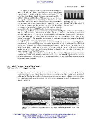
sive annealing conditions to achieve complete grain growth. Small grains can be seen in the bottom
of 0.18 µm trenches after a 3 min anneal at 250°C (Fig. 16.6). Complete grain growth is observed in
the same features after 30 s at 400°C. If adhesion between the barrier and the seed layer is poor, high-
temperature annealing can cause copper to delaminate (de wet, agglomerate), leaving voids at the
bottom of features. 35,36 The annealing process must be integrated in conjunction with the barrier and
the seed deposition process to prevent void formation.
Uniformity of ECD copper films must be examined both locally (feature scale) and globally
(wafer scale). Global uniformity of the film across the wafer is critical to ensure that all portions of
the wafer are cleared of the excess copper material during the CMP process at the same time. If a
portion of the wafer clears before the rest, the excessive polishing in that area can lead to dishing and
erosion problems. For optimum performance, the final profile of the deposited film should match the
removal rate profile of the CMP system.
13
The bottom-up fill process leads to excess plating above features. In extreme cases, the bump
can be more than twice the thickness of blanket areas. This is very difficult to planarize and leads to
residual copper after CMP (see Fig. 16.7). Bump formation can be significantly reduced with leveler
chemistries or pulse plating.
16.5 ADDITIONAL CONSIDERATIONS
FOR COPPER ECD PROCESSING
In addition to process integration, there are several other factors that must be considered when using
copper in chip production. The plating chemistry must be maintained within specification at all times
to ensure consistent yield. Chemical waste must be classified and treated appropriately. In addition
to this, measures must be taken to ensure that copper contamination does not affect other areas of the
fabrication facility.
FIGURE 16.6 FIB images of 0.18 trenches (cut lengthwise) that have been annealed at 250°C and
400°C.
Downloaded from Digital Engineering Library @ McGraw-Hill (www.digitalengineeringlibrary.com)
Copyright © 2004 The McGraw-Hill Companies. All rights reserved.
Any use is subject to the Terms of Use as given at the website.