
Page 110 - The Art and Science of Analog Circuit Design
P. 110
William H, Gross
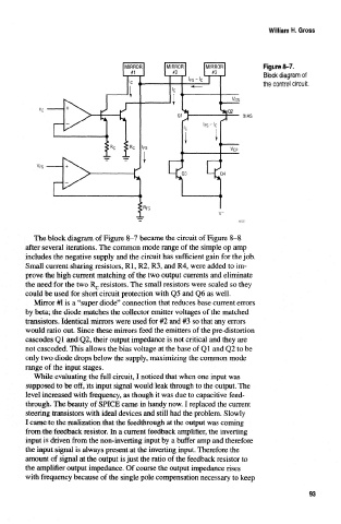
Figure 8-7.
Block diagram of
the control circuit.
BIAS
The block diagram of Figure 8-7 became the circuit of Figure 8-8
after several iterations. The common mode range of the simple op amp
includes the negative supply and the circuit has sufficient gain for the job.
Small current sharing resistors, Rl, R2, R3, and R4, were added to im-
prove the high current matching of the two output currents and eliminate
the need for the two R c resistors. The small resistors were scaled so they
could be used for short circuit protection with Q5 and Q6 as well.
Mirror #1 is a "super diode" connection that reduces base current errors
by beta; the diode matches the collector emitter voltages of the matched
transistors. Identical mirrors were used for #2 and #3 so that any errors
would ratio out. Since these mirrors feed the emitters of the pre-distortion
cascodes Ql and Q2, their output impedance is not critical and they are
not cascoded. This allows the bias voltage at the base of Ql and Q2 to be
only two diode drops below the supply, maximizing the common mode
range of the input stages.
While evaluating the full circuit, I noticed that when one input was
supposed to be off, its input signal would leak through to the output. The
level increased with frequency, as though it was due to capacitive feed-
through. The beauty of SPICE came in handy now. I replaced the current
steering transistors with ideal devices and still had the problem. Slowly
I came to the realization that the feedthrough at the output was coming
from the feedback resistor. In a current feedback amplifier, the inverting
input is driven from the non-inverting input by a buffer amp and therefore
the input signal is always present at the inverting input. Therefore the
amount of signal at the output is just the ratio of the feedback resistor to
the amplifier output impedance. Of course the output impedance rises
with frequency because of the single pole compensation necessary to keep
93