
Page 549 - The Mechatronics Handbook
P. 549
0066_Frame_C20 Page 19 Wednesday, January 9, 2002 5:41 PM
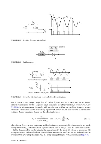
FIGURE 20.29 Thyristor driving a resistive load.
FIGURE 20.30 Snubber circuit.
FIGURE 20.31 Controlled (thyristor) and uncontrolled (diode) rectifications.
zero. A typical rate of voltage change that will induce thyristor turn-on is about 50 V/µs. To prevent
undesired conduction due to a large rate (high frequency) of voltage variation, a snubber circuit, see
Fig. 20.30, is often connected in parallel with the thyristor to filter out the high frequency voltage
variations. The snubber circuit is essentially a passive RC low-pass filter. The selection of the snubber
resistance R S and capacitance C S can use the following formula:
2
C S = ------------------------------- - and R S = 2 ----- – R L (20.12)
V Amax
L L
(
2
L L dV/dt) max C S
where R L and L L are the load inductance and load resistance, respectively. V Amax is the maximum anode
voltage and (dV/dt) max is the maximum expected rate of raise of voltage across the anode and cathode.
Unlike diodes used in rectifier circuits that can only rectify the input AC voltage to an average DC
voltage, thyristors can be used to build controlled rectifiers that can rectify AC sources and modulate the
average output DC voltage by modulating the firing timing of the gate voltage/current, see Fig. 20.31.
©2002 CRC Press LLC