
Page 551 - The Mechatronics Handbook
P. 551
0066_Frame_C20 Page 21 Wednesday, January 9, 2002 5:41 PM
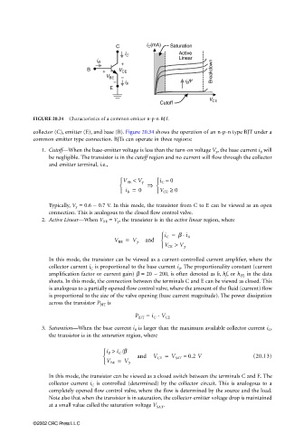
FIGURE 20.34 Characteristics of a common emitter n-p-n BJT.
collector (C), emitter (E), and base (B). Figure 20.34 shows the operation of an n-p-n type BJT under a
common emitter type connection. BJTs can operate in three regions:
1. Cutoff—When the base-emitter voltage is less than the turn-on voltage V γ , the base current i B will
be negligible. The transistor is in the cutoff region and no current will flow through the collector
and emitter terminal, i.e.,
V BE < V γ i C ≈ 0
⇒
i B = 0 V CE ≥ 0
Typically, V γ = 0.6 − 0.7 V. In this mode, the transistor from C to E can be viewed as an open
connection. This is analogous to the closed flow control valve.
2. Active Linear—When V BE = V γ , the transistor is in the active linear region, where
⋅
i C = β i B
V BE = V γ and
V CE > V γ
In this mode, the transistor can be viewed as a current-controlled current amplifier, where the
collector current i C is proportional to the base current i B . The proportionality constant (current
amplification factor or current gain) β = 20 ~ 200, is often denoted as h, hf, or h FE in the data
sheets. In this mode, the connection between the terminals C and E can be viewed as closed. This
is analogous to a partially opened flow control valve, where the amount of the fluid (current) flow
is proportional to the size of the valve opening (base current magnitude). The power dissipation
across the transistor P BJT is
P = i · V
BJT C CE
3. Saturation—When the base current i B is larger than the maximum available collector current i C ,
the transistor is in the saturation region, where
i B > i C /β
and V CE = V SAT ≈ 0.2 V (20.13)
V BE = V γ
In this mode, the transistor can be viewed as a closed switch between the terminals C and E. The
collector current i C is controlled (determined) by the collector circuit. This is analogous to a
completely opened flow control valve, where the flow is determined by the source and the load.
Note also that when the transistor is in saturation, the collector-emitter voltage drop is maintained
at a small value called the saturation voltage V SAT .
©2002 CRC Press LLC