
Page 555 - The Mechatronics Handbook
P. 555
0066_Frame_C20 Page 25 Wednesday, January 9, 2002 5:41 PM
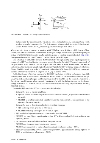
FIGURE 20.41 MOSFET as a voltage controlled switch.
In this mode, the transistor can be viewed as a closed switch between the terminals D and S with
a voltage controlled resistance R ON . The drain current i D is controlled (determined) by the drain
circuit. At rate current, the V DS drop during saturation ranges from 2 to 5 V.
When operating in the enhancement mode, a MOSFET behaves very similar to a BJT. Instead of base
current, the MOSFET behavior is determined by the gate voltage. When carefully controlling the gate
voltage of a MOSFET, the transistor can be made to operate as a voltage controlled switch (Fig. 20.41)
that operates between the cutoff (point A) and the Ohmic (point B) region.
One advantage of a MOSFET device is that the MOSFET has significantly larger input impedance as
compared to BJT. This simplifies the circuit that is needed to drive the MOSFET since the magnitude of
the gate current is not a factor. This also implies that a MOSFET is much more efficient than BJTs as
well as it can be switching at a much higher frequency. Typical MOSFET switching frequency is between
20 and 200 kHz, which is an order of magnitude higher than BJTs. Power MOSFETs can carry drain
currents up to several hundreds of amperes and V DS up to around 500 V.
Field effect is one of the key reasons why MOSFET has better switching performance than BJT.
However, static field is also one of its main failure modes. MOSFETs are very sensitive to static voltage.
Since the oxide insulating the gate and the substrate is only a thin film (in the order of a fraction to a
few micrometer), high static voltage can easily break down the oxide insulation. A typical gate breakdown
voltage is about 50 V. Therefore, static electricity control or insulation is very important when handling
MOSFET devices.
Comparing BJT with MOSFET, we can conclude the following:
• Both can be used as current amplifiers.
• BJT is a current-controlled amplifier where the collector current i C is proportional to the base
current i B .
• MOSFET is a voltage-controlled amplifier where the drain current i D is proportional to the
square of the gate voltage V G .
• Both can be used as three terminal switches or voltage inverters.
• BJT: switching circuit give rise to TTL logics.
• MOSFET: switching circuit give rise to CMOS logics.
• BJT usually has larger current capacity than similar sized MOSFET.
• MOSFET has much higher input impedance than BJT and is normally off, which translates to less
operating power.
• MOSFETs are more easily fabricated into integrated circuit.
• MOSFETs are less prone to go into thermal runaway.
• MOSFETs are susceptible to static voltage (exceed gate breakdown voltage ∼50 V).
• BJT has been replaced by MOSFET in low-voltage (<500 V) applications and is being replaced by
IGBT in applications at voltages above 500 V.
©2002 CRC Press LLC