
Page 559 - The Mechatronics Handbook
P. 559
0066_Frame_C20 Page 29 Wednesday, January 9, 2002 5:41 PM
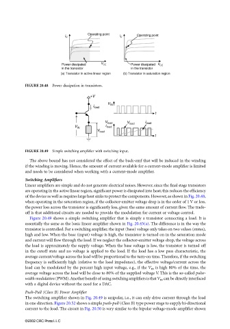
FIGURE 20.48 Power dissipation in transistors.
FIGURE 20.49 Simple switching amplifier with switching input.
The above bound has not considered the effect of the back-emf that will be induced in the winding
if the winding is moving. Hence, the amount of current available for a current-mode amplifier is limited
and needs to be considered when working with a current-mode amplifier.
Switching Amplifiers
Linear amplifiers are simple and do not generate electrical noises. However, since the final stage transistors
are operating in the active linear region, significant power is dissipated into heat; this reduces the efficiency
of the device as well as requires large heat sinks to protect the components. However, as shown in Fig. 20.48,
when operating in the saturation region, if the collector-emitter voltage drop is in the order of 1 V or less,
the power loss across the transistor is significantly less, given the same amount of current flow. The trade-
off is that additional circuits are needed to provide the modulation for current or voltage control.
Figure 20.49 shows a simple switching amplifier that is simply a transistor connecting a load. It is
essentially the same as the basic linear amplifier shown in Fig. 20.43(a). The difference is in the way the
transistor is controlled. For a switching amplifier, the input (base) voltage only takes on two values (states),
high and low. When the base (input) voltage is high, the transistor is turned on in the saturation mode
and current will flow through the load. If we neglect the collector-emitter voltage drop, the voltage across
the load is approximately the supply voltage. When the base voltage is low, the transistor is turned off
in the cutoff state and no voltage is applied to the load. If the load has a low pass characteristic, the
average current/voltage across the load will be proportional to the turn-on time. Therefore, if the switching
frequency is sufficiently high (relative to the load impedance), the effective voltage/current across the
load can be modulated by the percent high input voltage, e.g., if the V IN is high 80% of the time, the
average voltage across the load will be close to 80% of the supplied voltage V. This is the so-called pulse-
width modulation (PWM). Another benefit of using switching amplifiers is that V IN can be directly interfaced
with a digital device without the need for a DAC.
Push-Pull (Class B) Power Amplifier
The switching amplifier shown in Fig. 20.49 is unipolar, i.e., it can only drive current through the load
in one direction. Figure 20.52 shows a simple push-pull (Class B) type power stage to supply bi-directional
current to the load. The circuit in Fig. 20.50 is very similar to the bipolar voltage-mode amplifier shown
©2002 CRC Press LLC