
Page 554 - The Mechatronics Handbook
P. 554
0066_Frame_C20 Page 24 Wednesday, January 9, 2002 5:41 PM
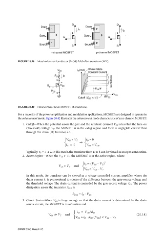
FIGURE 20.39 Metal-oxide-semiconductor (MOS) field effect transistor (FET).
FIGURE 20.40 Enhancement mode MOSFET characteristic.
For a majority of the power amplification and modulation applications, MOSFETs are designed to operate in
the enhancement mode. Figure 20.42 illustrates the enhancement mode characteristic of an n-channel MOSFET:
1. Cutoff—When the potential across the gate and the substrate (source) V GS is less that the turn-on
(threshold) voltage V T , the MOSFET is in the cutoff region and there is negligible current flow
through the drain (D) terminal, i.e.,
V GS < V T i D ≈ 0
⇒
i G = 0 V DS ≈ V DD
Typically, V T ≈ 1–2 V. In this mode, the transistor from D to S can be viewed as an open connection.
2. Active Region—When the V GS > V T , the MOSFET is in the active region, where
i D ∝ ( V GS – V T ) 2
V GS > V T and
V DS > V GS – V T
In this mode, the transistor can be viewed as a voltage-controlled current amplifier, where the
drain current i C is proportional to square of the difference between the gate-source voltage and
the threshold voltage. The drain current is controlled by the gate-source voltage V GS . The power
dissipation across the transistor P FET is
P FET = i · V DS
D
3. Ohmic State—When V GS is large enough so that the drain current is determined by the drain
source circuit, the MOSFET is in saturation and
i D = V DD /R D
and (20.14)
V GS >> V T
⋅
(
V DS ≈ i D R ON V DS ) < V GS – V T
©2002 CRC Press LLC