
Page 553 - The Mechatronics Handbook
P. 553
0066_Frame_C20 Page 23 Wednesday, January 9, 2002 5:41 PM
C C
Q1
Q1
b b
B B 1 1
b b
2 2
Q2
Q2
E E
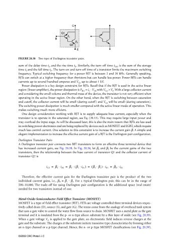
FIGURE 20.38 Two type of Darlington transistor pairs.
sum of the delay time t D and the rise time t R . Similarly, the turn-off time t OFF is the sum of the storage
time t S and the fall time t F . The turn-on and turn-off time of a transistor limits the maximum switching
frequency. Typical switching frequency for a power BJT is between 2 and 20 kHz. Generally speaking,
BJTs can switch at a higher frequency than thyristors but can handle less power. Power BJTs can handle
currents up to several hundred amperes and V CE up to about 1 kV.
Power dissipation is a key design constraint for BJTs. Recall that if the BJT is used in the active linear
region (linear amplifier), the power dissipation is P BJT = i C · V CE with V CE > V γ . With a large collector current
and considering the small volume and thermal mass of the device, the transistor is not very efficient when
operating in the active linear region. On the other hand, when the BJT is switching between saturation
and cutoff, the collector current will be small (during cutoff) and V CE will be small (during saturation).
The switching power dissipation is much smaller compared with the active linear mode of operation. This
makes switching much more efficient.
One design consideration working with BJT is to supply adequate base current, especially when the
transistor is to operate in the saturated region, see Eq. (20.13). This may require large input power and
may overload the input stage. As will be discussed later, this is also the main reason that BJTs are less used
in switching power electronics and are being replaced by devices such as MOSFET and IGBT, which require
much less control current. One solution to this constraint is to increase the current gain β. A simple and
elegant implementation to increase the effective current gain of a BJT is the Darlington pair configuration.
Darlington Transistor Pairs
A Darlington transistor pair connects two BJT transistors to form an effective three terminal device that
has increased current gain, see Fig. 20.38. In Fig. 20.38, let β 1 and β 2 be the current gains of the two
transistors, then the relationship between the base current of transistor Q1 and the collector current of
transistor Q2 is
i C2 = β 2 i B2 = β 2 ( β 1 i B1 ) = ( β 2 β 1 ) i B1 = β D i B1
⋅
⋅
⋅
⋅
⋅
⋅
Therefore, the effective current gain for the Darlington transistor pair is the product of the two
individual current gains, i.e., β D = β 1 · β 2 . For a typical Darlington pair, this can be in the range of
500–10,000. The trade-off for using Darlington pair configuration is the additional space (real estate)
needed for two transistors instead of one.
Metal-Oxide-Semiconductor Field Effect Transistor (MOSFET)
MOSFET is a type of field effect transistor (FET). FETs are voltage controlled three terminal devices respec-
tively called drain (D), source (S), and gate (G). The terms come from the analogy of overhead tank system
that uses a gate valve to control the water flow from source to drain. MOSFET uses a metal plate as the gate
terminal and it is insulated from the p- or n-type silicon substrate by a thin layer of oxide (see Fig. 20.39).
When a gate voltage V G is applied to the gate plate, an electrostatic field induces reverse charges at the
gate and the substrate. The charges at the substrate initiate transistor type characteristics by forming either
an n-type channel or a p-type channel. Hence, the n- or p-type MOSFET classifications (see Fig. 20.39).
©2002 CRC Press LLC