Page 121 - An Introduction to Microelectromechanical Systems Engineering
P. 121

100                     MEM Structures and Systems in Industrial and Automotive Applications
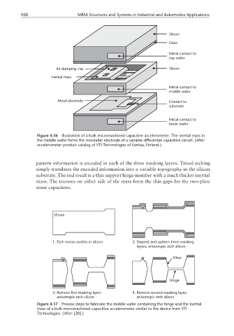


                                                                          Silicon
                                                                          Glass

                                                                          Metal contact to
                                                                          top wafer

                         Air damping vias                                 Silicon
                       Inertial mass

                                                                          Metal contact to
                                                                          middle wafer

                          Metal electrode                                 Contact to
                                                                          substrate


                                                                          Metal contact to
                                                                          lower wafer

                 Figure 4.16  Illustration of a bulk micromachined capacitive accelerometer. The inertial mass in
                 the middle wafer forms the moveable electrode of a variable differential capacitive circuit. (After:
                 accelerometer product catalog of VTI Technologies of Vantaa, Finland.)


                 pattern information is encoded in each of the three masking layers. Timed etching
                 simply translates the encoded information into a variable topography in the silicon
                 substrate. The end result is a thin support hinge member with a much thicker inertial
                 mass. The recesses on either side of the mass form the thin gaps for the two-plate
                 sense capacitors.


                        Silicon


                        1. Etch recess cavities in silicon  2. Deposit and pattern three masking
                                                            layers;  anisotropic etch silicon

                                                                            Mass


                                                                          Hinge

                        3. Remove first masking layer;    4. Remove second masking layer;
                         anisotropic etch silicon           anisotropic etch silicon
                 Figure 4.17  Process steps to fabricate the middle wafer containing the hinge and the inertial
                 mass of a bulk micromachined capacitive accelerometer similar to the device from VTI
                 Technologies. (After: [20].)
   116   117   118   119   120   121   122   123   124   125   126