
Page 28 - Analog and Digital Filter Design
P. 28
25
Introduction
The power dissipated at a resistive load is the product of voltage and current
averaged over one sine wave cycle. This is the r.m.s. voltage times the r.m.s.
current. No power is dissipated in a purely reactive load because over one coni-
plete sine wave cycle the product of voltage and current is zero. Instead, energy
is stored in capacitors and inductors, which is the reason for the phase differ-
ence between voltage and current at a reactive load.
Inductors have an impedance given by the expression X, = jwL. Capacitors have
an impedance given by the expression X, = l/jnC, which is equivalent to Xc =
-j/wC. The symbol '7'' indicates a phase shift of 90" (or -90" for the "-j" term).
This means that if a sinusoidal voltage is applied across a pure inductor. the
peak current flow occurs 1/4 cycle after the peak voltage is applied. The -j term
describing the capacitor's impedance means that the peak current flow through
a capacitor occurs '/J cycle before the peak voltage is applied. Because the voltage
and current are not in phase, the impedance is described as reactance rather than
as resistance.
Analog Filters
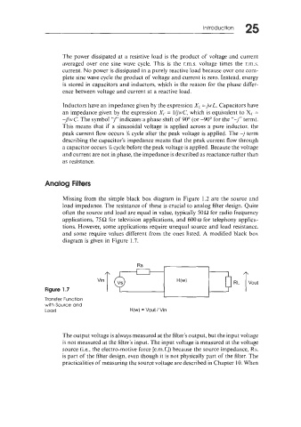
Missing from the simple black box diagram in Figure 1.2 are the source and
load impedance. The resistance of these is crucial to analog filter design. Quite
often the source and load are equal in value, typically 50Q for radio frequency
applications, 75 R for television applications, and 600 w for telephony applica-
tions. However, some applications require unequal source and load resistance.
and some require values different from the ones listed. A modified black box
diagram is given in Figure 1.7.
Vin 1 r-3 RL Tvout
Figure 1.7
Transfer Function
with Source and
Load H(w) = Vout / Vin
The output voltage is always measured at the filter's output, but the input voltage
is not measured at the filter's input. The input voltage is measured at the voltage
source (Le., the electro-motive force [e.m.f.]) because the source impedance, Rs,
is part of the filter design, even though it is not physically part of the filter. The
practicalities of measuring the source voltage are described in Chapter 10. When