
Page 94 - Automotive Engineering Powertrain Chassis System and Vehicle Body
P. 94
CH AP TER 4 .1 Digital engine control systems
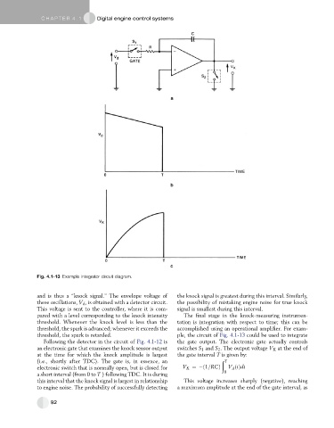
Fig. 4.1-13 Example integrator circuit diagram.
and is thus a ‘‘knock signal.’’ The envelope voltage of the knock signal is greatest during this interval. Similarly,
these oscillations, V d , is obtained with a detector circuit. the possibility of mistaking engine noise for true knock
This voltage is sent to the controller, where it is com- signal is smallest during this interval.
pared with a level corresponding to the knock intensity The final stage in the knock-measuring instrumen-
threshold. Whenever the knock level is less than the tation is integration with respect to time; this can be
threshold, the spark is advanced; whenever it exceeds the accomplished using an operational amplifier. For exam-
threshold, the spark is retarded. ple, the circuit of Fig. 4.1-13 could be used to integrate
Following the detector in the circuit of Fig. 4.1-12 is the gate output. The electronic gate actually controls
an electronic gate that examines the knock sensor output switches S 1 and S 2 . The output voltage V K at the end of
at the time for which the knock amplitude is largest the gate interval T is given by:
(i.e., shortly after TDC). The gate is, in essence, an ð T
electronic switch that is normally open, but is closed for V K ¼ ð1=RCÞ V ðtÞdt
d
a short interval (from 0 to T ) following TDC. It is during 0
this interval that the knock signal is largest in relationship This voltage increases sharply (negative), reaching
to engine noise. The probability of successfully detecting a maximum amplitude at the end of the gate interval, as
92