
Page 373 - Complete Wireless Design
P. 373
Support Circuit Design
372 Chapter Eight
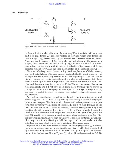
Figure 8.47 The series-pass regulator with feedback.
its forward bias so that this error detector/amplifier transistor will now con-
duct less. This forces Q ’s collector voltage to increase, which then forces the
2
base voltage of Q to rise, making this series-pass transistor conduct harder.
1
Now, increased current will flow through any load placed at the regulator’s
output, thus increasing the output voltage. Q ’s emitter is clamped at a refer-
2
ence voltage by the zener, with R setting the diode’s idling current, while the
5
collector resistor for Q and the base bias resistor for Q is supplied by R .
2 1 4
Three-terminal regulators (shown in Fig. 8.43) are, because of their low cost,
size, and weight, high efficiency, and great simplicity, the most common type
of regulator for almost any circuit or system requiring 3 A or less (much
higher currents are possible with the addition of external components). These
devices are integrated circuit regulators that include full internal current lim-
iting and thermal protection circuits, so if the IC’s internal power dissipation
rises excessively, the 3-T will shut itself down before burning out. As shown in
the figure, the 3-T circuit employs R and R to fix the output voltage level. R
1 2 2
can also be varied in order to change this output voltage for almost any
requirement.
Very efficient switching regulators are found in an increasing number of
power supplies. These devices regulate by outputting a variable-duty-cycle
pulse into a low-pass filter in step with the output load requirements, and per-
form this switching with speeds of between 20 and 500 kHz. Because of the
fast rise and fall times of these waveforms, however, strong switching noise
constituents will be produced within the regulator. These must be heavily fil-
tered to reduce excessive hash output into sensitive radio gear. Thus, their use
is still limited in certain communications gear, where designers may favor lin-
ear power supply regulators, such as the 3-T. If selected, switching power sup-
plies require not only filtering of all the input and output leads, but also
shielding and very short trace runs to minimize EMI generation.
Figure 8.48 is a common architecture for a switching regulator. Q , a switch-
1
ing pass transistor, receives pulses into its base from a VCO that is controlled
by a comparator. Q then outputs a switching voltage in step with these com-
1
mands into the lowpass filter of L and C , which filter the pulses into DC. By
1 1
Downloaded from Digital Engineering Library @ McGraw-Hill (www.digitalengineeringlibrary.com)
Copyright © 2004 The McGraw-Hill Companies. All rights reserved.
Any use is subject to the Terms of Use as given at the website.