
Page 374 - Complete Wireless Design
P. 374
Support Circuit Design
Support Circuit Design 373
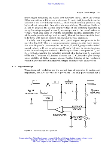
increasing or decreasing the pulse’s duty cycle into this LC filter, the average
DC output voltage will increase or decrease. D protects Q from the inductive
1 1
kickback of the stored charge within L , which would normally produce a very
1
high spike of voltage into the emitter during switching. The voltage divider of
R and R program the desired output voltage of the switching regulator by
1 2
using the voltage dropped across R as a comparison to the zener’s reference
2
voltage, which then turns on or off the comparator, and thus controls the VCO,
all depending on the voltage level across R . Most of the above circuit is found
2
in IC form, with built-in current-limiting and thermal protection.
A widely used integrated version, with typical support components, is dis-
played in Fig. 8.49. This is a common regulator arrangement in many produc-
tion switching-mode power supplies. As above, R and R program the desired
1 2
output voltage, with the voltage across R being fed back by the feedback line
2
to the internal comparator circuits. The low-pass filter is composed of L and
1
C , with D shunting the inductive kickback of a discharging L to ground
OUT 1 1
(when the IC switches off), instead of across the IC. C is used to give the reg-
1
ulator stability at higher current draws. Further filtering at the regulator’s
output may be required if undesirable ripple amplitudes are still present.
8.7.3 Regulator design
Three-terminal regulators are the easiest type of regulator to design and
implement, and are also the most prevalent. The only parts needed for a
Figure 8.48 Switching regulator operation.
Downloaded from Digital Engineering Library @ McGraw-Hill (www.digitalengineeringlibrary.com)
Copyright © 2004 The McGraw-Hill Companies. All rights reserved.
Any use is subject to the Terms of Use as given at the website.