
Page 156 -
P. 156
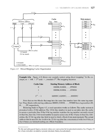
4.3 / ELEMENTS OF CACHE DESIGN 127

                               s + w


                                                  Cache                      Main memory
                  Memory address               Tag  Data                        WO
             Tag     Line    Word                                                W1
                                                                                 W2      B 0
                                                            L 0
           s – r     r       w                                                   W3


                                     s – r


                                                                          s
                                       w                    L                   W4j
             Compare                                         i            w    W(4j+1)   B j
                                                                               W(4j+2)
                                                                               W(4j+3)
                            (Hit in cache)
                    1 if match
                    0 if no match

                                                            L m–1
                 0 if match
                 1 if no match
                            (Miss in cache)
           Figure 4.9 Direct-Mapping Cache Organization


                                                                                5
                   Example 4.2a  Figure 4.10 shows our example system using direct mapping. In the ex-
                   ample, m =  16K =  2 and i =  j modulo 2 . The mapping becomes
                                    14
                                                     14
                                 Cache Line      Starting Memory Address of Block
                                     0             000000, 010000, Á ,  FF0000
                                     1             000004, 010004, Á ,  FF0004
                                     o                        o
                                  2 14  -  1      00FFFC, 01FFFC, Á ,  FFFFFC
                       Note that no two blocks that map into the same line number have the same tag num-
                   ber.Thus, blocks with starting addresses 000000, 010000, Á ,  FF0000 have tag numbers 00,
                   01, Á ,  FF, respectively.
                       Referring back to Figure 4.5, a read operation works as follows. The cache system is
                   presented with a 24-bit address. The 14-bit line number is used as an index into the cache
                   to access a particular line. If the 8-bit tag number matches the tag number currently stored
                   in that line, then the 2-bit word number is used to select one of the 4 bytes in that line. Oth-
                   erwise, the 22-bit tag-plus-line field is used to fetch a block from main memory.The actual
                   address that is used for the fetch is the 22-bit tag-plus-line concatenated with two 0 bits, so
                   that 4 bytes are fetched starting on a block boundary.


                  5 In this and subsequent figures, memory values are represented in hexadecimal notation. See Chapter 19
                  for a basic refresher on number systems (decimal, binary, hexadecimal).