
Page 375 - DSP Integrated Circuits
P. 375
360 Chapter 8 DSP Architectures
Most DSP routines are fairly small and can reside either in the on-chip pro-
gram memory or in a small external EPROM. Most DSP routines are hand-coded
to fully exploit the DSPs architectural features [6]—for example, to reduce the
inefficiencies associated with flushing long pipelines, unwinding short loops and
interleaving several independent loops to keep the pipelines full [22].
Branch instructions waste processing time in heavily pipelined architectures.
The typical solution is to use dedicated hardware that allows zero-overhead loop.
However, hardware support is often provided for only one loop due to the cost.
8.3.1 Harvard Architecture
In the classical von Neumann architecture the ALU and the control unit are con-
nected to a single memory that stores both the data values and the program
instructions. During execution, an instruction is read from the memory and
decoded, appropriate operands are fetched from the memory, and, finally, the
instruction is executed. The main disadvantage is that memory bandwidth
becomes the bottleneck in such an architecture.
The most common operation a standard DSP processor must be able to per-
form efficiently is multiply-and-accumulate. This operation should ideally be per-
formed in a single instruction cycle. This means that two values must be read from
memory and (depending on organization) one value must be written, or two or
more address registers must be updated, in that cycle. Hence, a high memory
bandwidth is just as important as a fast multiply-and-accumulate operation.
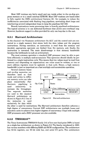
Several memory buses
and on-chip memories are
therefore used so that
reads and writes to differ-
ent memory units can take
place concurrently. Fur-
thermore, pipelining is
used extensively to
increase the throughput.
Two separate memories
are used in the classical
Harvard architecture as
shown in Figure 8.5. One of
the memories is used
exclusively for data while
the other is used for instructions. The Harvard architecture therefore achieves a
high degree of concurrency. Current DSP architectures use multiple buses and
execution units to achieve even higher degrees of concurrency. Chips with multiple
DSP processors and a RISC processor are also available.
8.3.2 TMS32010™
The Texas Instruments TMS32010 family [14] of low-cost fixed-point DSPs is based
on a single-bus architecture as shown in Figure 8.6. The family, introduced in 1983,
has various members with differing RAM and ROM configurations. The architecture
has 32-bit registers, one 16—bit wide bus, and serial I/O ports. This architecture