
Page 377 - DSP Integrated Circuits
P. 377
362 Chapter 8 DSP Architectures
The TMS320C25, which is pin-compatible with the TMS32020, is a 16-bit
fixed-point DSP with 32-bit registers. The chip uses a Harvard architecture and is
manufactured in a 1.8-um CMOS process. The current version can be clocked at 50
MHz. The instruction cycle time is 80 ns—i.e., 12.5 MIPS @ 50 MHz. The
TMS320C25 is available in a 68-pin PLCC package. Typical performance of the
TMS320C25 is as follows: An N-tap FIR filter requires N+8 clock cycles while N
second-order sections require 15A/+4 clock cycles. A 91-tap FIR filter can be exe-
cuted in 7.92 us and a sixth-order filter in 3.72 us. A 256-point and a 1024-point
FFT, without bit-reversal, take 1.8 and 15.6 ms, respectively.
The TMS320C50 is an enhanced version of the TMS320C25 with twice as
large a throughput. Distinguishing features are low loop overhead and 10 kwords
of on-chip RAM.
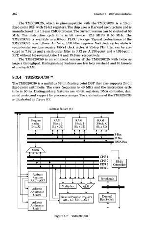
8.3.4 TMS320C30™
The TMS320C30 is a multibus 32-bit floating-point DSP that also supports 24-bit
fixed-point arithmetic. The clock frequency is 40 MHz and the instruction cycle
time is 50 ns. Distinguishing features are 40-bit registers, DMA controller, dual
serial ports, and support for processor arrays. The architecture of the TMS320C30
is illustrated in Figure 8.7.
Figure 8.7 TMS320C30