
Page 381 - DSP Integrated Circuits
P. 381
366 Chapter 8 DSP Architectures
of these assignments determine the communication requirement—i.e., communi-
cation channels and their bandwidth, etc. Hence, the minimum requirements are
specified in these design steps. Therefore, to each static schedule corresponds a
class of ideal multiprocessor architectures.
An ideal DSP architecture belongs to a class of architectures that implements
the static schedule. An ideal architecture has processing elements that can exe-
cute the operations according to the schedule and is supported with appropriate
communication channels and memories.
Note that there may be several architectures that implement a given sched-
ule, and that a new class of architectures is obtained if the schedule is changed.
Algorithms that require dynamic scheduling lead to architectures that either must
handle worst-case situations or are optimized in a statistical sense. However, the
execution time must be predictable since the sample period constraint must be
met in hard real-time applications [13]. The latter type of architectures are there-
fore difficult to use.
8.4.1 Processing Elements
Processing elements (PEs) usually perform simple, memoryless mappings of the
input values to a single output value. The arithmetic operations commonly used in
DSP algorithms are
Add/sub, add/sub-and-shift
Multiply, multiply-and-accumulate
Vector product
Two-port adaptor
Butterfly
We will reserve the more general term processor to denote a PE with its inter-
nal memory and control circuitry. Hence, a processor is able to perform a task
independently or otner processors.
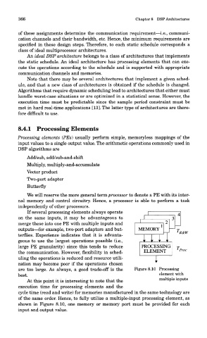
If several processing elements always operate
on the same inputs, it may be advantageous to
merge these into one PE with multiple inputs and
outputs—for example, two-port adaptors and but-
terflies. Experience indicates that it is advanta-
geous to use the largest operations possible (i.e.,
large PE granularity) since this tends to reduce
the communication. However, flexibility in sched-
uling the operations is reduced and resource utili-
zation may become poor if the operations chosen
are too large. As always, a good trade-off is the Figure 8.10 Processing
best. element with
At mis point it is interesting to note tnat tne multiple inputs
execution time for processing elements and the
cycle time (read and write) for memories manufactured in the same technology are
of the same order. Hence, to fully utilize a multiple-input processing element, as
shown in Figure 8.10, one memory or memory port must be provided for each
input and output value.