
Page 378 - DSP Integrated Circuits
P. 378
8.3 Standard DSP Architectures 363
An JV-tap FIR filter requires N+5 clock cycles while N second-order sections
require 6AT+24 clock cycles. A 91-tap FIR filter can be executed in 4.0 us and a
sixth-order filter in 1.8 us. A 256-point and a 1024-point FFT, without bit-reversal,
take 0.68 and 1.97 ms, respectively.
8.3.5 TMS320C40™
The TMS320C40 floating-point DSP provides extensive parallel processing sup-
port through six buffered byte-wide 20 Mb/s links and a six-channel DMA copro-
cessor. It runs at 50 MHz and can perform up to eight operations per instruction
cycle, which corresponds to 200 MFLOPS. The DMA coprocessor can perform up to
75 MFLOPS.
The TMS320C40 presents a more conventional architecture, where parallelism
is achieved by pipelining and the ability to execute certain instructions in parallel.
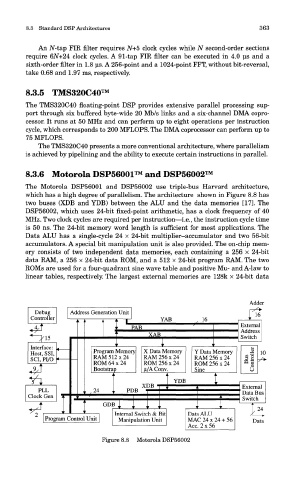
8.3.6 Motorola DSP56001™ and DSP56002™
The Motorola DSP56001 and DSP56002 use triple-bus Harvard architecture,
which has a high degree of parallelism. The architecture shown in Figure 8.8 has
two buses (XDB and YDB) between the ALU and the data memories [17]. The
DSP56002, which uses 24-bit fixed-point arithmetic, has a clock frequency of 40
MHz. Two clock cycles are required per instruction—i.e., the instruction cycle time
is 50 ns. The 24-bit memory word length is sufficient for most applications. The
Data ALU has a single-cycle 24 x 24-bit multiplier-accumulator and two 56-bit
accumulators. A special bit manipulation unit is also provided. The on-chip mem-
ory consists of two independent data memories, each containing a 256 x 24-bit
data RAM, a 256 x 24-bit data ROM, and a 512 x 24-bit program RAM. The two
ROMs are used for a four-quadrant sine wave table and positive Mu- and A-law to
linear tables, respectively. The largest external memories are 128k x 24-bit data
Figure 8.8 Motorola DSP56002