
Page 380 - DSP Integrated Circuits
P. 380
8.4 Ideal DSP Architectures 365
faces are provided. The on-chip memory consists of two independent memories,
each containing a 512 x 32-bit data RAM, a 512 x 32-bit data ROM, and a 512 x 32-
bit program RAM. The two ROMs are used for two-quadrant sine and cosine wave
tables. The DSP96001 is available in a 163-pin pin-grid array package.
The DSP96002 is a dual-port version of the DSP96001. The two expansion
ports effectively double the off-chip bus bandwidth [18]. The size of the on-chip
program RAM has been increased from 512 to 1024 words. The DSP96002 can per-
form up to 10 operations simultaneously. The peak performance is 200 MOPS and
50 MFLOP @ a 40-MHz clock frequency. Typical power consumption is less than 1
W. The DSP96002 is available in a 223-pin pin-grid array package. Typical perfor-
mance of the DSP96001 is as follows: An N-tap FIR filter requires N+7 clock cycles
while N second-order sections in direct form II require 5N+5 clock cycles. A 91-tap
FIR filter can be executed in 4.9 us and a sixth-order filter in 1.0 us. A 1024-point
FFT, without bit-reversal, takes 1.04 ms, while the DSP96002 requires less than
0.8 ms.
8.4 IDEAL DSP ARCHITECTURES
At the architectural level, the main interest is the overall organization of the sys-
tem which is described in terms of the high-level primitives: processors, memories,
communication channels, and control [13]. These primitives are characterized by
parameters such as memory capacity, access time, word length, transmission
rates, and processor execution time. At this level, the designer is also interested in
the global data flow between the high-level primitives in the system. The objective
is to estimate system performance and identify potential bottlenecks in data
transmission within the system. At the end of the architectural design phase, tim-
ing relations between the hardware components are of more interest. Also test pat-
tern generation and fault simulation are a concern at this stage of the system
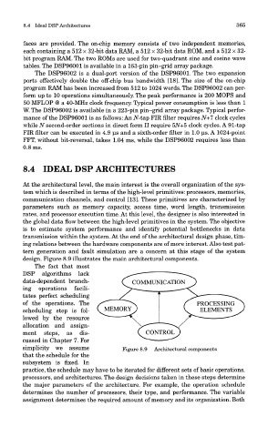
design. Figure 8.9 illustrates the main architectural components.
The fact that most
DSP algorithms lack
data-dependent branch-
ing operations facili-
tates perfect scheduling
of the operations. The
scheduling step is fol-
lowed by the resource
allocation and assign-
ment steps, as dis-
cussed in Chapter 7. For
simplicity we assume Figure 8.9 Architectural components
that the schedule for the
subsystem is fixed. In
practice, the schedule may have to be iterated for different sets of basic operations,
processors, and architectures. The design decisions taken in these steps determine
the major parameters of the architecture. For example, the operation schedule
determines the number of processors, their type, and performance. The variable
assignment determines the required amount of memory and its organization. Both