
Page 376 - DSP Integrated Circuits
P. 376
8.3 Standard DSP Architectures 361
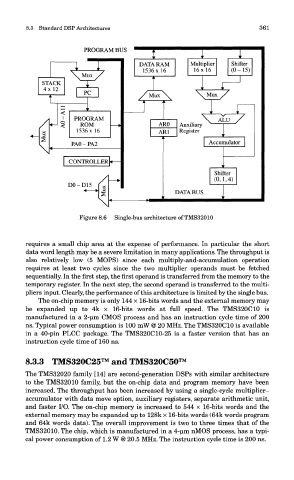
Figure 8.6 Single-bus architecture of TMS32010
requires a small chip area at the expense of performance. In particular the short
data word length may be a severe limitation in many applications. The throughput is
also relatively low (5 MOPS) since each multiply-and-accumulation operation
requires at least two cycles since the two multiplier operands must be fetched
sequentially. In the first step, the first operand is transferred from the memory to the
temporary register. In the next step, the second operand is transferred to the multi-
pliers input. Clearly, the performance of this architecture is limited by the single bus.
The on-chip memory is only 144 x 16-bits words and the external memory may
be expanded up to 4k x 16-bits words at full speed. The TMS320C10 is
manufactured in a 2-um CMOS process and has an instruction cycle time of 200
ns. Typical power consumption is 100 mW @ 20 MHz. The TMS320C10 is available
in a 40-pin PLCC package. The TMS320C10-25 is a faster version that has an
instruction cycle time of 160 ns.
8.3.3 TMS320C25™ and TMS320C50™
The TMS32020 family [14] are second-generation DSPs with similar architecture
to the TMS32010 family, but the on-chip data and program memory have been
increased. The throughput has been increased by using a single-cycle multiplier-
accumulator with data move option, auxiliary registers, separate arithmetic unit,
and faster I/O. The on-chip memory is increased to 544 x 16-bits words and the
external memory may be expanded up to 128k x 16-bits words (64k words program
and 64k words data). The overall improvement is two to three times that of the
TMS32010. The chip, which is manufactured in a 4-um nMOS process, has a typi-
cal power consumption of 1.2 W @ 20.5 MHz. The instruction cycle time is 200 ns.