
Page 403 - DSP Integrated Circuits
P. 403
388 Chapter 9 Synthesis of DSP Architectures
implementations useful in applications with small work loads. In the second case
each process is assigned to a dedicated PE. This approach trades large power con-
sumption and chip area for high throughput.
9.2 MAPPING OF DSP ALGORITHMS
ONTO HARDWARE
The majority of conventional architectures proposed for digital signal processing
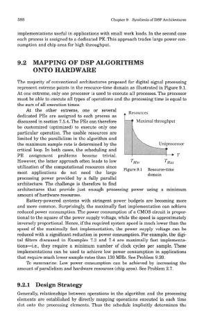
represent extreme points in the resource-time domain as illustrated in Figure 9.1.
At one extreme, only one processor is used to execute all processes. The processor
must be able to execute all types of operations and the processing time is equal to
the sum of all execution times.
At the other extreme, one or several
dedicated PEs are assigned to each process as
discussed in section 7.5.4. The PEs can therefore
be customized (optimized) to execute only one
particular operation. The usable resources are
limited by the parallelism in the algorithm anc
the maximum sample rate is determined by the
critical loop. In both cases, the scheduling and
PE assignment problems become trivial
However, the latter approach often leads to lo\v
utilization of the computational resources since
Figure 9.1 Resource-time
most applications do not need the large
domain
processing power provided by a fully parallel
architecture. The challenge is therefore to find
architectures that provide just enough processing power using a minimum
amount of hardware resources.
Battery-powered systems with stringent power budgets are becoming more
and more common. Surprisingly, the maximally fast implementation can achieve
reduced power consumption. The power consumption of a CMOS circuit is propor-
tional to the square of the power supply voltage, while the speed is approximately
inversely proportional. Hence, if the required system speed is much lower than the
speed of the maximally fast implementation, the power supply voltage can be
reduced with a significant reduction in power consumption. For example, the digi-
tal filters discussed in Examples 7.3 and 7.4 are maximally fast implementa-
tions—i.e., they require a minimum number of clock cycles per sample. These
implementations can be used to achieve low power consumption in applications
that require much lower sample rates than 130 MHz. See Problem 9.20.
To summarize: Low power consumption can be achieved by increasing the
amount of parallelism and hardware resources (chip area). See Problem 2.7.
9.2.1 Design Strategy
Generally, relationships between operations in the algorithm and the processing
elements are established by directly mapping operations executed in each time
slot onto the processing elements. Thus the schedule implicitly determines the