
Page 422 - DSP Integrated Circuits
P. 422
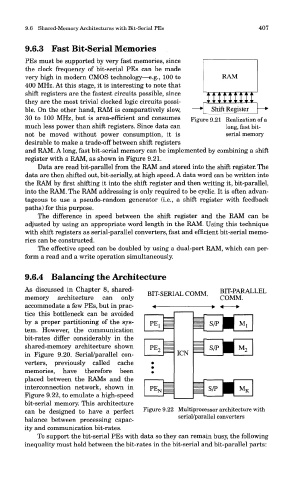
9.6 Shared-Memory Architectures with Bit-Serial PEs                  407


        9.6.3 Fast Bit-Serial Memories
        PEs must be supported by very fast memories, since
        the clock frequency of bit-serial PEs can be made
        very high in modern CMOS technology—e.g., 100 to
        400 MHz. At this stage, it is interesting to note that
        shift registers are the fastest circuits possible, since
        they are the most trivial clocked logic circuits possi-
        ble. On the other hand, RAM is comparatively slow,
        30 to 100 MHz, but is area-efficient and consumes  Figure 9.21 Realization of a
        much less power than shift registers. Since data can       long, fast bit-
        not be moved without power consumption, it is              serial memory
        desirable to make a trade-off between shift registers
        and RAM. A long, fast bit-serial memory can be implemented by combining a shift
        register with a RAM, as shown in Figure 9.21.
            Data are read bit-parallel from the RAM and stored into the shift register. The
        data are then shifted out, bit-serially, at high speed. A data word can be written into
        the RAM by first shifting it into the shift register and then writing it, bit-parallel,
        into the RAM. The RAM addressing is only required to be cyclic. It is often advan-
        tageous to use a pseudo-random generator (i.e., a shift register with feedback
        paths) for this purpose.
            The difference in speed between the shift register and the RAM can be
        adjusted by using an appropriate word length in the RAM. Using this technique
        with shift registers as serial-parallel converters, fast and efficient bit-serial memo-
        ries can be constructed.
            The effective speed can be doubled by using a dual-port RAM, which can per-
        form a read and a write operation simultaneously.


        9.6.4 Balancing the Architecture
        As discussed in Chapter 8, shared-
        memory architecture    can only
        accommodate a few PEs, but in prac-
        tice this bottleneck can be avoided
        by a proper partitioning of the sys-
        tem. However, the communication
        bit-rates differ considerably in the
        shared-memory architecture shown
        in Figure 9.20. Serial/parallel con-
        verters, previously called cache
        memories, have therefore    been
        placed between the RAMs and the
        interconnection network, shown in
        Figure 9.22, to emulate a high-speed
        bit-serial memory. This architecture
        can be designed to have a perfect  Figure 9.22 Multiprocessor architecture with
                                                     serial/parallel converters
        balance between processing capac-
        ity and communication bit-rates.
            To support the bit-serial PEs with data so they can remain busy, the following
        inequality must hold between the bit-rates in the bit-serial and bit-parallel parts: