
Page 423 - DSP Integrated Circuits
P. 423
408 Chapter 9 Synthesis of DSP Architectures
where N s is the number of bit-serial PEs, and Tp^ s is their clock frequency. Thus, by
choosing an appropriate word length, WM, in the memories, a sufficiently high bit-
rate can be obtained. To avoid fractions of data words at the same address, the mem-
ory word length, WM, must be chosen so that
The maximum number of PEs in one system is limited either by the parallel-
ism in the algorithm or by the data word length. We have
Typically, we have 4Tpg s ~ TM- Thus, one system can typically support 2 to 3
PEs, since normal data word lengths are in the range 16 to 24 bits. In general, it is
possible to use different data word lengths and to use multiple word lengths in dif-
ferent PEs and subsystems. Note that the factor 2, in Equation (9.10), can be
removed by using two sets of memories. Hence, the number of PEs in one system
can be increased to about W^/4, or 4 to 6 PEs. Note that this represents a signifi-
cant amount of processing capacity.
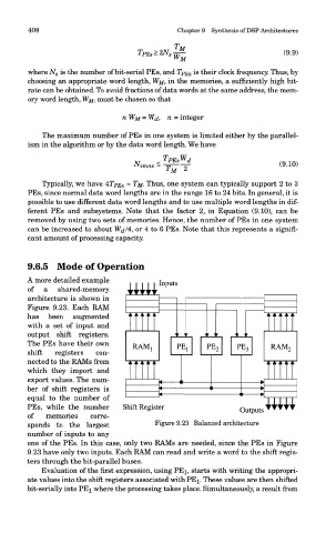
9.6.5 Mode of Operation
A more detailed example
of a shared-memory
architecture is shown in
Figure 9.23. Each RAM
has been augmented
with a set of input and
output shift registers.
The PEs have their own
shift registers con-
nected to the RAMs from
which they import and
export values. The num-
ber of shift registers is
equal to the number of
PEs, while the number
of memories corre-
sponds to the largest Figure 9.23 Balanced architecture
number of inputs to any
one of the PEs. In this case, only two RAMs are needed, since the PEs in Figure
9.23 have only two inputs. Each RAM can read and write a word to the shift regis-
ters through the bit-parallel buses.
Evaluation of the first expression, using PE^, starts with writing the appropri-
ate values into the shift registers associated with PEi. These values are then shifted
bit-serially into PEi where the processing takes place. Simultaneously, a result from