
Page 421 - DSP Integrated Circuits
P. 421
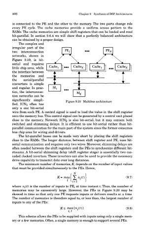
406                                     Chapter 9 Synthesis of DSP Architectures


        is connected to the PE and the other to the memory. The two parts change role
        every PE cycle. The cache memories provide a uniform access pattern to the
        RAMs. The cache memories are simple shift registers that can be loaded and read
        bit-parallel. In section 9.6.4 we will show that a perfectly balanced architecture
        can be obtained by a proper design.
            The complex and
        irregular part of the
        two interconnection
        networks, shown in
        Figure 9.19, is bit-
        serial and requires
        little chip area, while
        the interface between
        the memories and
        the    serial/parallel
        converters is simple
        and regular. In prac-
        tice, the interconnec-
        tion networks can be
        significantly simpli-
                                        Figure 9.20 Multibus architecture
        fied. ICNi often has
        only a one bit-serial
        wire irom each PE. A control signal is used to load the value in the shut register
        onto the memory bus. This control signal can be generated by a control unit placed
        close to the memory. Network ICN2 is also bit-serial, but it may contain both
        switched and shimming delays. It is efficient to use bit-serial rather than bit-
        parallel communication for the main part of the system since the former consumes
        less chip area for wiring and drivers.
            The bit-parallel buses can be made very short by placing the shift registers
        close to the RAMs. The longer distance, between shift register and PE, uses bit-
        serial communication and requires only two wires. Moreover, shimming delays are
        often needed between the shift registers and the PEs to synchronize different bit-
        streams. A bit-serial shimming delay (shift register stage) is essentially two cas-
        caded clocked inverters. These inverters can also be used to provide the necessary
        drive capability to transmit data over long distances.
            The minimum number of memories, K, depends on the number of input values
        that must be provided simultaneously to the PEs. Hence,


        where ni(t) is the number of inputs to PEj at time instant t. Thus, the number of
        memories may be excessively large. However, the PEs in Figure 9.20 may be
        skewed in time so that only one PE requests inputs or delivers results at a time.
        The number of memories is therefore equal to, or less than, the largest number of
        inputs to any of the PEs:


            This scheme allows the PEs to be supplied with inputs using only a single mem-
        ory or a few memories. Often, a single memory is enough to support several PEs.