
Page 424 - DSP Integrated Circuits
P. 424
9.6 Shared-Memory Architectures with Bit-Serial PEs 409
the previous operation will appear at the output of PEi, since pipelining is inherent
in the bit-serial PEs. The result is shifted into the shift registers, at the bottom of
Figure 9.23, and finally written into the appropriate RAM. These two operations
take two RAM cycles: one read and one write. In the next RAM cycle the input val-
ues to PE2 can be written into its shift registers and so on. The operational scheme
for all PEs is the same, but the PEs are skewed in time by two clock cycles, as shown
in Figure 9.24. The operation of the system is fully synchronous.
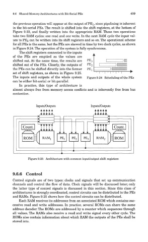
me snitt registers connected to tne inputs
of the PEs are emptied as the values are
shifted out. At the same time, the results are
shifted out of the PEs. Clearly, the outputs of
the PEs can be shifted directly into the former
set of shift registers, as shown in Figure 9.25.
The inputs and outputs of the whole system Figure 9.24 Scheduling of the PEs
can be either bit-serial or bit-parallel.
In practice, this type of architecture is
almost always free from memory access conflicts and is inherently free from bus
contention.
Figure 9.25 Architecture with common input/output shift registers
9.6.6 Control
Control signals are of two types: clocks and signals that set up communication
channels and control the flow of data. Clock signals will be discussed later; only
the latter type of control signals is discussed in this section. Since this class of
architectures is strongly coordinated, control circuits can be distributed to the PEs
and RAMs. Figure 9.25 shows how the control circuits can be distributed.
Each RAM receives its addresses from an associated ROM which contains suc-
cessive read and write addresses. In practice, several ROMs can share the same
address decoder. The ROMs are addressed by a counter which sequences through
all values. The RAMs also receive a read and write signal every other cycle. The
ROMs also contain information about which RAM the outputs of the PEs shall be
stored into.